
Datasheet

LTC490
2
490fb
(Note 1)
Supply Voltage (V
CC
) ............................................... 12V
Driver Input Currents ........................... –25mA to 25mA
Driver Input Voltages ...................... –0.5V to V
CC
+ 0.5V
Driver Output Voltages .......................................... ±14V
Receiver Input Voltages ......................................... ±14V
Receiver Output Voltages ............... –0.5V to V
CC
+ 0.5V
Operating Temperature Range
LTC490C ................................................ 0°C to 70°C
LTC490I............................................. –40°C to 85°C
Storage Temperature Range ................. –65°C to 150°C
Lead Temperature (Soldering, 10 sec).................. 300°C
T
JMAX
= 125°C, θ
JA
= 100°C/W (N8)
T
JMAX
= 150°C, θ
JA
= 150°C/W (S8)
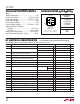
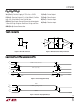
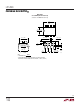
N8 PACKAGE
8-LEAD PDIP
S8 PACKAGE
8-LEAD PLASTIC SO
1
2
3
4
8
7
6
5
TOP VIEW
V
CC
R
D
GND
A
B
Z
Y
R
D
ORDER PART
NUMBER
S8 PART MARKING
LTC490CN8
LTC490CS8
LTC490IN8
LTC490IS8
490
490I
The ● denotes the specificatiions which apply over the full
operating temperature range, otherwise specifications are at T
A
= 25°C. V
CC
= 5V ±5%
SYMBOL PARAMETER CONDITIONS MIN TYP MAX UNITS
V
OD1
Differential Driver Output Voltage (Unloaded) I
O
= 0
●
5V
V
OD2
Differential Driver Output Voltage (with Load) R = 50Ω (RS422)
●
2V
R = 27Ω (RS485) (Figure 1)
●
1.5 5 V
∆V
OD
Change in Magnitude of Driver Differential Output R = 27Ω or R = 50Ω (Figure 1)
●
0.2 V
Voltage for Complementary Output States
V
OC
Driver Common Mode Output Voltage R = 27Ω or R = 50Ω (Figure 1)
●
3V
∆ V
OC
Change in Magnitude of Driver Common Mode R = 27Ω or R = 50Ω (Figure 1)
●
0.2 V
Output Voltage for Complementary Output States
V
IH
Input High Voltage (D)
●
2.0 V
V
IL
Input Low Voltage (D)
●
0.8 V
l
IN1
Input Current (D)
●
±2 µA
l
IN2
Input Current (A, B) V
CC
= 0V or 5.25V V
IN
= 12V
●
1mA
V
IN
= –7V
●
–0.8 mA
V
TH
Differential Input Threshold Voltage for Receiver –7V ≤ V
CM
≤ 12V
●
–0.2 0.2 V
∆V
TH
Receiver Input Hysteresis V
CM
= 0V
●
70 mV
V
OH
Receiver Output High Voltage I
O
= –4mA, V
ID
= 0.2V
●
3.5 V
V
OL
Receiver Output Low Voltage I
O
= 4mA, V
ID
= – 0.2V
●
0.4 V
I
OZR
Three-State Output Current at Receiver V
CC
= Max 0.4V ≤ V
O
≤ 2.4V
●
±1 µA
I
CC
Supply Current No Load; D = GND or V
CC
●
300 500 µA
R
IN
Receiver Input Resistance –7V ≤ V
O
≤ 12V
●
12 kΩ
I
OSD1
Driver Short-Circuit Current, V
OUT
= High V
O
= – 7V
●
100 250 mA
I
OSD2
Driver Short-Circuit Current, V
OUT
= Low V
O
= 12V
●
100 250 mA
I
OSR
Receiver Short-Circuit Current 0V ≤ V
O
≤ V
CC
●
785mA
I
OZ
Driver Three-State Output Current V
O
= –7V to 12V
●
±2 ±200 µA
ABSOLUTE AXI U RATI GS
WWWU
Consult LTC Marketing for parts specified with wider operating temperature ranges.
PACKAGE/ORDER I FOR ATIO
UU
W
DC ELECTRICAL CHARACTERISTICS