
Datasheet


5
LTC490
490fb
–V
O
LTC490 • F03
D
3V
0V
1.5V
t
PLH
1.5V
V
DIFF
= V(Y) – V(Z)
V
O
80%
20%
50%
10%
Z
Y
t
SKEW
t
r
f = 1MHz : t
r
≤ 10ns : t
f
≤ 10ns
90%
50%
t
PHL
t
f
V
O
t
SKEW
1/2 V
O
1/2 V
O
UU
U
PI FU CTIO S
V
CC
(Pin 1): Positive Supply; 4.75V ≤ V
CC
≤ 5.25V.
R (Pin 2): Receiver Output. If A > B by 200mV, R will be
high. If A < B by 200mV, then R will be low.
D (Pin 3): Driver Input. A low on D forces the driver outputs
Y low and Z high. A high on D will force Y high and Z low.
GND (Pin 4): Ground Connection.
Y (Pin 5): Driver Output.
Z (Pin 6): Driver Output.
B (Pin 7): Receiver Input.
A (Pin 8): Receiver Input.
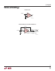
Figure 4. Receiver Propagation Delays
Figure 3. Driver Propagation Delays
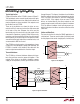
Figure 1. Driver DC Test Load Figure 2. Driver/Receiver Timing Test Circuit
TEST CIRCUITS
LTC490 • F01
Y
Z
R
R
V
OD2
V
OC
LTC490 • F02
DRIVER
D
Y
Z
RECEIVER
R
DIFF
A
B 15pF
C
L1
C
L2
R
SWITCHI G TI E WAVEFOR S
UWW
V
OL
LTC490 • F04
A-B
V
OD2
0V
t
PLH
0V
OUTPUT
V
OH
1.5V
f = 1MHz ; t
r
≤ 10ns : t
f
≤ 10ns
t
PHL
–V
OD2
1.5V
INPUT
R