
Datasheet

1
LTC491
491fa
■
Low Power: I
CC
= 300µA Typical
■
Designed for RS485 or RS422 Applications
■
Single 5V Supply
■
–7V to 12V Bus Common Mode Range
Permits ±7V Ground Difference Between Devices
on the Bus
■
Thermal Shutdown Protection
■
Power-Up/-Down Glitch-Free Driver Outputs Permit
Live Insertion or Removal of Package
■
Driver Maintains High Impedance in Three-State or
with the Power Off
■
Combined Impedance of a Driver Output and
Receiver Allows up to 32 Transceivers on the Bus
■
70mV Typical Input Hysteresis
■
28ns Typical Driver Propagation Delays with 5ns
Skew for 2.5MB Operation
■
Pin Compatible with the SN75180
■
Available in 14-Lead PDIP and SO Packages
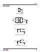
Differential Driver and
Receiver Pair
The LTC
®
491 is a low power differential bus/line trans-
ceiver designed for multipoint data transmission standard
RS485 applications with extended common mode range
(12V to –7V). It also meets the requirements of RS422.
The CMOS design offers significant power savings over its
bipolar counterpart without sacrificing ruggedness against
overload or ESD damage.
The driver and receiver feature three-state outputs, with
the driver outputs maintaining high impedance over the
entire common mode range. Excessive power dissipation
caused by bus contention or faults is prevented by a
thermal shutdown circuit which forces the driver outputs
into a high impedance state.
The receiver has a fail safe feature which guarantees a high
output state when the inputs are left open.
Both AC and DC specifications are guaranteed from 0°C to
70°C and 4.75V to 5.25V supply voltage range.
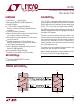
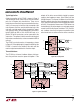
■
Low Power RS485/RS422 Transceiver
■
Level Translator
LTC491 • TA01
120Ω 120Ω
120Ω 120Ω
4000 FT 24 GAUGE TWISTED PAIR
4000 FT 24 GAUGE TWISTED PAIR
RECEIVER
LTC491
DRIVER
RECEIVER
LTC491
DRIVER
R
D
R
D
5
2
11
12
10
9
4
DE
3
REB
DE
REB
FEATURES
DESCRIPTIO
U
APPLICATIO S
U
TYPICAL APPLICATIO
U
, LTC and LT are registered trademarks of Linear Technology Corporation.