
Datasheet

3
LTC491
491fa
SYMBOL PARAMETER CONDITIONS MIN TYP MAX UNITS
t
PLH
Driver Input to Output R
DIFF
= 54Ω, C
L1
= C
L2
= 100pF ● 10 30 50 ns
t
PHL
Driver Input to Output ● 10 30 50 ns
t
SKEW
Driver Output to Output ● 5ns
t
r
, t
f
Driver Rise or Fall Time ● 51525 ns
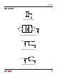
t
ZH
Driver Enable to Output High C
L
= 100pF (Figures 4, 6) S2 Closed ● 40 70 ns
t
ZL
Driver Enable to Output Low C
L
= 100pF (Figures 4, 6) S1 Closed ● 40 70 ns
t
LZ
Driver Disable Time From Low C
L
= 15pF (Figures 4, 6) S1 Closed ● 40 70 ns
t
HZ
Driver Disable Time From High C
L
= 15pF (Figures 4, 6) S2 Closed ● 40 70 ns
t
PLH
Receiver Input to Output R
DIFF
= 54Ω, C
L1
= C
L2
= 100pF ● 40 70 150 ns
t
PHL
Receiver Input to Output ● 40 70 150 ns
t
SKD
t
PLH
– t
PHL
Differential Receiver Skew ● 13 ns
t
ZL
Receiver Enable to Output Low C
L
= 15pF (Figures 3, 8) S1 Closed ● 20 50 ns
t
ZH
Receiver Enable to Output High C
L
= 15pF (Figures 3, 8) S2 Closed ● 20 50 ns
t
LZ
Receiver Disable From Low C
L
= 15pF (Figures 3, 8) S1 Closed ● 20 50 ns
t
HZ
Receiver Disable From High C
L
= 15pF (Figures 3, 8) S2 Closed ● 20 50 ns
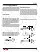
S
U
GC CHARA TERIST
ICS
WI
TCH
I
(Figures 2, 5)
(Figures 2, 7)
Note 3: All typicals are given for V
CC
= 5V and temperature = 25°C.Note 1: Absolute Maximum Ratings are those values beyond which the life
of the device may be impaired.
Note 2: All currents into device pins are positive; all currents out of device
pins are negative. All voltages are referenced to device ground unless
otherwise specified.
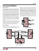
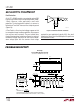
NC (Pin 1): Not Connected.
R (Pin 2): Receiver Output. If the receiver output is enabled
(REB low), then if A > B by 200mV, R will be high. If A < B
by 200mV, then R will be low.
REB (Pin 3): Receiver Output Enable. A low enables the
receiver output, R. A high input forces the receiver output
into a high impedance state.
DE (Pin 4): Driver Output Enable. A high on DE enables the
driver outputs, Y and Z. A low input forces the driver
outputs into a high impedance state.
D (Pin 5): Driver Input. If the driver outputs are enabled
(DE high), then a low on D forces the driver outputs Y low
and Z high. A high on D will force Y high and Z low.
GND (Pin 6): Ground Connection.
GND (Pin 7): Ground Connection.
NC (Pin 8): Not Connected.
Y (Pin 9): Driver Output.
Z (Pin 10): Driver Output.
B (Pin 11): Receiver Input.
A (Pin 12): Receiver Input.
NC (Pin 13): Not Connected.
V
CC
(Pin 14): Positive Supply; 4.75V ≤ V
CC
≤ 5.25V.
The ● denotes the specifications which apply over the full operating
temperature range, otherwise specifications are at T
A
= 25°C. V
CC
= 5V ±5%
UU
U
PI FU CTIO S