
Datasheet


LTC6090
1
6090fa
Typical applicaTion
FeaTures DescripTion
140V CMOS Rail-to-Rail
Output, Picoamp Input
Current Op Amp
The LTC
®
6090 is a high voltage precision operational
amplifier. The low noise, low bias current input stage is
ideal for high gain configurations. The LTC6090 has low
input offset voltage, a rail-to-rail output stage, and can be
run from a single 140V or split ±70V supplies.
The LTC6090 is internally protected against overtempera-
ture conditions. A thermal warning output, TFLAG, goes
active when the die temperature approaches 150°C. The
output stage can be turned off with the output disable pin
OD. By tying the OD pin to the thermal warning output,
the part will disable the output stage when it is out of the
safe operating area. These pins easily interface to any
logic family.
The LTC6090 is unity gain stable with up to a 200pF output
capacitor. A wide input and output common mode range
along with many features makes the LTC6090 useful for
many high voltage applications.
The LTC6090 is available in an 8-lead SO and 16-lead
TSSOP with exposed pad for low thermal resistance.
L, LT, LT C, LT M, Linear Technology and the Linear logo are registered trademarks of Linear
Technology Corporation. All other trademarks are the property of their respective owners.
140V
P-P
Sine Wave Output
applicaTions
n
Supply Range: ±4.75V to ±70V (140V)
n
0.1Hz to 10Hz Noise: 3.5μV
P-P
n
Input Bias Current: 50pA
n
Low Offset Voltage: 1.6mV Maximum
n
Rail-to-Rail Output Stage
n
Output Sink and Source 10mA
n
10MHz Gain Bandwidth Product
n
19V/µs Slew Rate
n
11nV/√Hz Noise Density
n
Thermal Shutdown
n
Available in Thermally Enhanced SOIC-8E or
TSSOP-16E Packages
n
ATE
n
Piezo Drivers
n
Photodiode Amplifier
n
High Voltage Regulators
n
Optical Networking
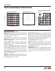
High Voltage DAC Buffer Application
V
OUT
= ±70V
6090 TA01a
–
+
LTC6090
453k
10pF
70V
3V
–70V
16.2k
16.9k
V
REF
= 2.5V
LTC2641D
IN
16
25µs/DIV
80
60
40
20
0
–20
–40
–60
–80
6090 TA01b
OUTPUT VOLTAGE (V)