
Datasheet


LTC6102
LTC6102-1/LTC6102HV
20
6102fe
For more information www.linear.com/LTC6102
applicaTions inForMaTion
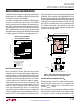
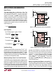
–INF
V
REG
0.1µF
–INS
6102 F11
R
IN
+
=
R
IN
–
–
R
SENSE
LTC6102-1
R
OUT
V
OUT
V
+
LOAD
R
BIAS
2.7M
R
SENSE
V
+
V
–
OUT
+IN
EN
R
IN
–
R
IN
+
–
+
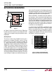
Figure 11
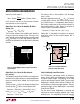
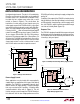
Figure 12. LTC6102-1 V
REG
Voltage During
Bypass Capacitor Discharge when Disabled
pin. Figure 11 shows the LTC6102-1 with a 2.7M pull-up
resistor to limit the current to less than 20µA with a 60V
supply, which is enough to satisfy the input bias current
requirement.
Start-Up Current
The start-up current of the LTC6102 when the part is
powered on or enabled (LTC6102-1) consists of three
parts: the first is the current necessary to charge the
V
REG
bypass capacitor, which is nominally 0.1µF. Since the
V
REG
voltage charges to approximately 4.5V below the V
+
voltage, this can require a significant amount of start-up
current. The second source is the active supply current of
the LTC6102 amplifier, which is not significantly greater
during start-up than during normal operation. The third
source is the output current of the LTC6102, which upon
start-up may temporarily drive the output high. This could
cause milliamps of output current (limited mostly by the
input resistor R
IN
) to flow into the output resistor and/or
the output limiting ESD structure in the LTC6102. This is
a temporary condition which will cease when the LTC6102
amplifier settles into normal closed-loop operation.
When the LTC6102-1 is disabled, the internal amplifier is
also shut down, which means that the discharge rate of
the 0.1µF capacitor is very low. This is significant when the
LTC6102-1 is disabled to save power, because the recharg
-
ing of the 0.1µF capacitor is a significant portion of the
overall power consumed in startup. Figure 12 shows the
discharge rate of the 0.1
µF capacitor after the L
TC6102-1
is shut down at room temperature.
In a system where the LTC6102-1 is disabled for short
periods, the start-up power (and therefore the average
power) can be reduced since the V
REG
bypass capacitor
is never significantly discharged. The time required to
charge the V
REG
capacitor will also be reduced, allowing
the LTC6102-1 to start-up more quickly.
TIME (ms)
–2
0
ENABLE VOLTAGE (V)
V
REG
VOLTAGE (V)
0.25
0.75
1.00
1.25
10
2.25
6102 F12
0.50
4
0
12
6
2
14
8 16
1.50
1.75
2.00
7.4
7.5
7.7
7.8
7.9
8.3
7.6
8.0
8.1
8.2
V
REG
EN
T
A
= 25°C
V
+
= 12V