
Datasheet


LTC6102
LTC6102-1/LTC6102HV
15
6102fe
For more information www.linear.com/LTC6102
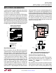
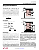
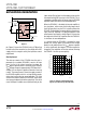
Figure 5. Second Input R Minimizes
Error Due to Input Bias Current
–INF
V
REG
0.1µF
–INS
6102 F05
R
IN
+
=
R
IN
–
–
R
SENSE
LTC6102
R
OUT
V
OUT
V
+
LOAD
R
SENSE
–
+
V
+
V
–
OUT
+IN
R
IN
–
R
IN
+
applicaTions inForMaTion
For instance if I
BIAS
is 1nA and R
OUT
is 10k, the output
error is –10µV.
Note that in applications where R
SENSE
≈ R
IN
, I
B
(+) causes
a voltage offset in R
SENSE
that cancels the error due to
I
B
(–) and E
OUT(IBIAS)
≈ 0. In applications where R
SENSE
<
R
IN
, the bias current error can be similarly reduced if an
external resistor R
IN
(+) = (R
IN
– R
SENSE
) is connected as
shown in Figure 5. Under both conditions:
E
OUT(IBIAS)
= ± R
OUT
• I
OS
; I
OS
= I
B
(+) – I
B
(–)
Adding R
IN
+
as described will maximize the dynamic
range of the circuit. For less sensitive designs, R
IN
+
is
not necessary.
Ideally, the circuit output is:
VV
R
R
VRI
OUT SENSE
OUT
IN
SENSESENSE SENSE
==
•; •
In this case, the only error is due to resistor mismatch,
which provides an error in gain only.
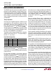
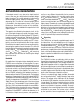
Output Error, E
OUT
, Due to the Amplifier DC Offset
Voltage, V
OS
E
OUT(VOS)
= V
OS
• (R
OUT
/R
IN
)
The DC offset voltage of the amplifier adds directly to
the value of the sense voltage, V
SENSE
. This error is very
small (3µV typ) and may be ignored for reasonable values
of R
IN
. See Figure 4. For very high dynamic range, this
offset can be calibrated in the system due to its extremely
low drift.
INPUT VOLTAGE (V)
OUTPUT ERROR (%)
100
10
1
0.1
0.01
0.001
0.0001
6102 F04
0.00001 0.0001 0.001 0.01 0.1 1
FOR A 500µΩ SHUNT
V
IN
= 100mV, I
SHUNT
= 200A
ERROR DUE TO V
OS
IS 6mA
V
IN
= 10µV
Figure 4. LTC6102 Output Error Due to Typical Input Offset
vs Input Voltage
Output Error, E
OUT
, Due to the Bias Currents,
I
B
(+) and I
B
(–)
The input bias current of the LTC6102 is vanishingly small.
However, for very high resolution, or at high temperatures
where I
B
increases due to leakage, the current may be
significant.
The bias current I
B
(+) flows into the positive input of the
internal op amp. I
B
(–) flows into the negative input.
E
OUT(IBIAS)
= R
OUT
((I
B
(+) • (R
SENSE
/R
IN
) – I
B
(–))
Since I
B
(+) ≈ I
B
(–) = I
BIAS
, if R
SENSE
<< R
IN
then,
E
OUT(IBIAS)
≈ –R
OUT
• I
BIAS
Clock Feedthrough, Input Bias Current
The LTC6102 uses auto-zeroing circuitry to achieve an
almost zero DC offset over temperature, sense voltage,
and power supply voltage. The frequency of the clock
used for auto-zeroing is typically 10kHz. The term clock
feedthrough is broadly used to indicate visibility of this
clock frequency in the op amp output spectrum. There are
typically two types of clock feedthrough in auto zeroed
amps like the LTC6102.
The first form of clock feedthrough is caused by the
settling of the internal sampling capacitor and is input
referred; that is, it is multiplied by the internal loop gain