
Datasheet


LTC6240/LTC6241/LTC6242
21
624012fe
The op amp’s good input offset voltage match and low
input bias current means that the typical differential output
offset voltage is less than 40µV. A noise spectrum plot of
the differential output is shown in Figure 5.
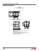
The guard ring should extend as far as necessary to shield
the high impedance signal from any and all leakage paths.
Figure 6 shows the use of a guard ring on the LTC6241 in
a unity gain confi guration. In this case the guard ring is
connected to the output and is shielding the high impedance
noninverting input from V
–
. Figure 7 shows the inverting
gain confi guration.
A Digitally Programmable AC Difference Amplifi er
The LTC6241 confi gured as a difference amplifi er, can be
combined with a programmable gain amplifi er (PGA) to
obtain a low noise high speed programmable difference
amplifi er. Figure 8 shows the LTC6241 based as a single-
supply AC amplifi er. One LTC6241 op amp is used at the
circuit’s input as a standard four resistor difference amplifi er.
Figure 5. Differential Output Noise
Achieving Low Input Bias Current
The DD package is leadless and makes contact to the PCB
beneath the package. Solder fl ux used during the attach-
ment of the part to the PCB can create leakage current
paths and can degrade the input bias current performance
of the part. All inputs are susceptible because the backside
paddle is connected to V
–
internally. As the input voltage
changes or if V
–
changes, a leakage path can be formed
and alter the observed input bias current. For lowest bias
current, use the LTC6240/LTC6241 in the SO-8 and provide
a guard ring around the inputs that are tied to a potential
near the input voltage.
Layout Considerations and a PCB Guard Ring
In high source impedance applications such as pH probes,
photodiodes, strain gauges, et cetera, the low input bias
current of these parts requires a clean board layout to
minimize additional leakage current into a high impedance
signal node. A mere 100G of PC board resistance
between a 5V supply trace and an input trace adds 50pA
of leakage current, far greater then the input bias current
of the operational amplifi er. A guard ring around the high
impedance input traces driven by a low impedance source
equal to the input voltage prevents such leakage problems.
Figure 6. Sample Layout. Unity Gain Confi guration, Using Guard
Ring to Shield High Impedance Input from Board Leakage
Figure 7. Sample Layout. Inverting Gain Confi guration, Using
Guard Ring to Shield High Impedance Input from Board Leakage
APPLICATIONS INFORMATION
FREQUENCY (kHz)
020 6010 40 8030 7050 90 100
DIFFERENTIAL OUTPUT VOLTAGE DENSITY (nV/√Hz)
140
60
80
100
120
0
20
40
6241 F05
V
S
= ±2.5V
T
A
= 25°C
–3dB BW = 80kHz
LTC6241 S8
R
OUT
+
IN
–
IN
+
V
–
LEAKAGE
CURRENT
NO LEAKAGE
CURRENT
GUARD
RING
NO SOLDER MASK
OVER THE GUARD RING
LTC6241 F06
LTC6241 S8
LTC6241 F07
R
R
OUT
+
IN
–
IN
+
V
–
V
IN
GND