
Datasheet


LTC6244
15
6244fb
Amplifi er Characteristics
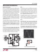
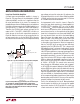
Figure 1 is a simplifi ed schematic of the LTC6244, which
has a pair of low noise input transistors M1 and M2. A
simple folded cascode Q1, Q2 and R1, R2 allow the input
stage to swing to the negative rail, while performing level
shift to the Differential Drive Generator. Low offset voltage
is accomplished by laser trimming the input stage.
Capacitor C1 reduces the unity cross frequency and im-
proves the frequency stability without degrading the gain
bandwidth of the amplifi er. Capacitor C
M
sets the overall
amplifi er gain bandwidth. The differential drive generator
supplies signals to transistors M3 and M4 that swing the
output from rail-to-rail.
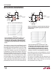
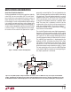
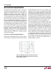
The photo of Figure 2 shows the output response to an
input overdrive with the amplifi er connected as a voltage
follower. If the negative going input signal is less than
a diode drop below V
–
, no phase inversion occurs. For
input signals greater than a diode drop below V
–
, limit the
current to 3mA with a series resistor R
S
to avoid phase
inversion.
The input common mode voltage range extends from
V
–
to V
+
– 1.5V. In unity gain voltage follower applications,
exceeding this range by applying a signal that reaches 1V
from the positive supply rail can create a low level instability
at the output. Loading the amplifi er with several hundred
micro-amps will reduce or eliminate the instability.
ESD
The LTC6244 has reverse-biased ESD protection diodes on
all input and outputs as shown in Figure 1. These diodes
protect the amplifi er for ESD strikes to 4kV. If these pins
are forced beyond either supply, unlimited current will
fl ow through these diodes. If the current transient is less
than 1 second and limited to one hundred milliamps or
less, no damage to the device will occur.
The amplifi er input bias current is the leakage current of
these ESD diodes. This leakage is a function of the tem-
perature and common mode voltage of the amplifi er, as
shown in the Typical Performance Chacteristics.
Noise
The LTC6244 exhibits low 1/f noise in the 0.1Hz to 10Hz
region. This 1.5µV
P-P
noise allows these op amps to be
used in a wide variety of high impedance low frequency
applications, where Zero-Drift amplifi ers might be inap-
propriate due to their input sampling characteristic.
In the frequency region above 1kHz the LTC6244 also
shows good noise voltage performance. In this frequency
region, noise can easily be dominated by the total source
Figure 1. Simplifi ed Schematic
Figure 2. Unity Gain Follower Test Circuit
APPLICATIONS INFORMATION
R2
6244 F01
V
IN
+
I
TAIL
V
IN
–
V
O
V
+
V
+
V
–
V
–
V
–
CM
DESD5
DIFFERENTIAL
DRIVE
GENERATOR
BIAS
DESD6
V
+
DESD2
V
+
DESD4
V
–
DESD1
V
–
DESD3
R1
Q1
M2M1
M3
M4
C1
Q2
+2.5V
R
S
0Ω
–2.5V
6244 F02
+
–
1/2
LTC6244
V
IN
V
OUT
V
OUT
AND V
IN
OF FOLLOWER WITH LARGE INPUT OVERDRIVE
V
+
2.5V
V
–
–2.5V