
Datasheet

LTC6252/LTC6253/LTC6254
13
625234fc
APPLICATIONS INFORMATION
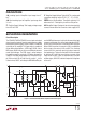
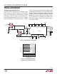
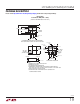
Circuit Description
The LTC6252/LTC6253/LTC6254 have an input and output
signal range that extends from the negative power supply
to the positive power supply. Figure 1 depicts a simplified
schematic of the amplifier. The input stage is comprised
of two differential amplifiers, a PNP stage, Q1/Q2, and an
NPN stage, Q3/Q4 that are active over different common
mode input voltages. The PNP stage is active between
the negative supply to nominally 1.2V below the positive
supply. As the input voltage approaches the positive sup-
ply, the transistor Q5 will steer the tail current, I
1
, to the
current mirror, Q6/Q7, activating the NPN differential pair
and the PNP pair becomes inactive for the remaining input
common mode range. Also, at the input stage, devices Q17
to Q19 act to cancel the bias current of the PNP input pair.
When Q1/Q2 are active, the current in Q16 is controlled to
be the same as the current in Q1 and Q2. Thus, the base
current of Q16 is nominally equal to the base current of
the input devices. The base current of Q16 is then mirrored
by devices Q17 to Q19 to cancel the base current of the
input devices Q1/Q2. A pair of complementary common
emitter stages, Q14/Q15, enable the output to swing from
rail-to-rail.
Figure 1. LTC6252/LTC6253/LTC6254 Simplified Schematic Diagram
–IN: Inverting Input of Amplifier. Input range from V
–
to V
+
.
+IN: Non-Inverting Input of Amplifier. Input range from
V
–
to V
+
.
V
+
: Positive Supply Voltage. Total supply voltage ranges
from 2.5V to 5.25V.
V
–
: Negative Supply Voltage. Typically 0V. This can be made
a negative voltage as long as 2.5V ≤ (V
+
– V
–
) ≤ 5.25V.
SHDN: Active Low Shutdown. Threshold is typically 1.1V
referenced to V
–
. Floating this pin will turn the part on.
OUT: Amplifier Output. Swings rail-to-rail and can typically
source/sink over 90mA of current at a total supply of 5V.
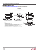
PIN FUNCTIONS
625234 F01
Q15
ESDD5
Q14
C2
C1
BUFFER
AND
OUTPUT BIAS
R5R4
Q13
Q12
I
3
V
–
+
C
C
Q8
R3
Q11
Q9
Q10
R2R1
Q2Q1Q3Q4
I
1
+
I
2
+
V
BIAS
Q5
Q6Q19
Q7
D8
D7
Q18
Q17
D6
D5
ESDD2
V
–
ESDD1
V
+
ESDD4
V
–
ESDD3
V
+
Q16
V
–
V
+
+IN
–IN
ESDD6
OUT