
Datasheet

LTC6252/LTC6253/LTC6254
17
625234fc
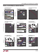
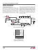
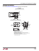
Low Noise Gain Block Using Channels in Parallel
Figure 5 shows the LTC6254 configured as a low noise
gain block. By configuring each channel as a gain of 10
block and putting all four gain blocks in parallel, the input
referred noise can be reduced significantly. 22Ω resistors
are hooked up to the outputs of each of the channels to
ensure even distribution of load currents.For a total sup-
ply current of 13.2mA, measured input referred noise
density (including contributions from the resistors) be-
tween 100kHz and 10MHz was less than 1.6nV/√Hz, with
input referred noise density at 1 MHz being 1.5nV/√Hz.
The measured –3dB frequency was 37MHz for a load
resistance of 1k.
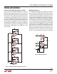
TYPICAL APPLICATIONS
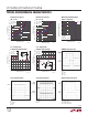
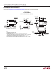
Multiplexing Channels
The LTC6252 and LTC6253 are available with shutdown
pins in the SOT-23 and MS10 packages. While this allows
for reduced power consumption, it also makes the parts
suitable for high output impedance applications such as
muxing. During shutdown, the bases of the amplifier’s
output channels are hard tied to their emitters in order to
minimize leakage. Figure 6 shows the LTC6253 applied as a
mux, with the outputs simply shorted together. Depending
on which device is powered, either the V
A
or the V
B
input
is buffered to V
OUT
. The MOSFET Q1 provides a simple
logic inversion, so that pulling the gate high selects the
B path while the FET drain goes low shutting down the A
path. R3 is provided to speed up the drain rise time. The
LTC6253 turn-on time is longer than the turn-off time
(3.5µs vs < 2µs) avoiding cross conduction in the output
Figure 5. Low Noise Gain Block Using Parallel Channels
Figure 6. Multiplexing Channels
¼ LTC6254
+
–
1pF
2.5V
–2.5V
900Ω
100Ω
22Ω
¼ LTC6254
+
–
1pF
900Ω
100Ω
22Ω
¼ LTC6254
+
–
1pF
900Ω
100Ω
22Ω
¼ LTC6254
+
–
1pF
900Ω
100Ω
V
IN
22Ω
V
OUT
625234 F05
625234 F06
+
–
5V
SHDNA
SHDNB
V
A
½ LTC6253
R1
330Ω
+
–
V
B
5V
Q1
2N7002
SEL_B
½ LTC6253
R2
330Ω
R3
20k
V
OUT