
Datasheet


LTC6409
12
6409fa
resistor mismatch can make the apparent voltage offset
of the amplifier appear worse than specified.
The apparent input referred offset induced by feedback
factor mismatch is derived from Equation (3):
V
OSDIFF(APPARENT)
≈ (V
CM
– V
OCM
) • Δb
Using the LTC6409 in a single 5V supply application with
0.1% resistors, the input common mode grounded, and
the V
OCM
pin biased at 1.25V, the worst case mismatch
can induce 1.25mV of apparent offset voltage.
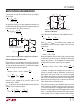
Noise and Noise Figure
The LTC6409’s differential input referred voltage and current
noise densities are 1.1nV/√Hz and 8.8pA/√Hz, respectively.
In addition to the noise generated by the amplifier, the
surrounding feedback resistors also contribute noise. A
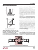
simplified noise model is shown in Figure 4. The output
noise generated by both the amplifier and the feedback
components is given by the equation:
e
no
=
e
ni
• 1+
R
F
R
I
2
+ 2 • i
n
• R
F
( )
2
+
2 • e
nRI
•
R
F
R
I
2
+ 2 • e
nRF
2
If the circuits surrounding the amplifier are well balanced,
common mode noise (e
nVOCM
) of the amplifier does not
appear in the differential output noise equation given above.
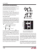
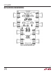
A plot of this equation and a plot of the noise generated
by the feedback components for the LTC6409 are shown
in Figure 5.
The LTC6409’s input referred voltage noise contributes
the equivalent noise of a 75Ω resistor. When the feedback
network is comprised of resistors whose values are larger
than this, the output noise is resistor noise and amplifier
current noise dominant. For feedback networks consist-
ing of resistors with values smaller than 75Ω, the output
noise is voltage noise dominant (see Figure 5).
Lower resistor values always result in lower noise at the
penalty of increased distortion due to increased loading
by the feedback network on the output. Higher resistor
values will result in higher output noise, but typically im-
proved distortion due to less loading on the output. For
this reason, when LTC6409 is configured in a differential
gain of 1, using feedback resistors of at least 150Ω is
recommended.
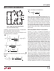
To calculate noise figure (NF), a source resistance and the
noise it generates should also come into consideration.
Figure 6 shows a noise model for the amplifier which
includes the source resistance (R
S
). To generalize the
applicaTions inForMaTion
Figure 4. Simplified Noise Model
–
+
e
no
2
R
F
V
OCM
e
nRI
2
R
F
R
I
R
I
e
nRF
2
e
nRI
2
e
ni
2
e
nRF
2
i
n+
2
i
n–
2
6409 F04
Figure 5. LTC6409 Output Noise vs Noise
Contributed by Feedback Network Alone
R
I
= R
F
(Ω)
NOISE DENSITY (nV/√Hz)
6409 F05
1000
100
10
1
0.1
10 1000 10000100
TOTAL (AMPLIFIER AND
FEEDBACK NETWORK)
OUTPUT NOISE
FEEDBACK
NETWORK
NOISE