
Datasheet

LTC6602
18
6602fc
APPLICATIONS INFORMATION
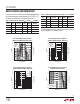
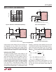
Figure 8. Distortion vs Common Mode Input Voltage (3V) Figure 9. Distortion vs Common Mode Input Voltage (5V)
Input Common Mode and Differential Voltage Range
The input signal range extends from zero to the V+
IN
sup-
ply voltage. This input supply can be tied to V+
A
and V+
D
,
or driven up to 5.5V for increased input common mode
voltage range. Figures 8 and 9 show the distortion of the
filter versus common mode input voltage with a 1.5V
P-P
differential input signal.
For best performance, the inputs should be driven dif-
ferentially. For single ended signals, connect the unused
input to V
OCM
(Pin 3) or to a quiet DC reference voltage.
To achieve the best distortion performance, the input
signal should be centered around the DC voltage of the
unused input.
Refer to the Typical Performance Characteristics section
to estimate the distortion for a given input level.
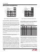
Dynamic Input Impedance
The unique input sampling structure of the LTC6602 has a
dynamic input impedance which depends on the configura-
tion and the clock frequency. This dynamic input impedance
has both a differential component and a common mode
component. The common mode input impedance is a
function of the clock frequency and the control bit LPF1.
The differential input impedance is a function of the clock
frequency and the control bits LPF1, GAIN1 and GAIN0.
Table 4 shows the typical input impedances for a clock
frequency of 90MHz. These input impedances are all pro-
portional to 1/f
CLK
, so if the clock frequency were reduced
by half to 45MHz, the impedances would be doubled. The
typical part to part variation in dynamic input impedance
for a given clock frequency is –20% to +35%.
Table 4. Differential, Common Mode Input Impedances,
f
CLK
= 90MHz
GAIN1
GAIN0
LPF1
DIFFERENTIAL INPUT
IMPEDANCE (kΩ)
COMMON MODE INPUT
IMPEDANCE (kΩ)
0 0 0 16 20
0 0 1 6 6.7
0 1 0 8 20
0 1 1 2.8 6.7
1 0 0 2.6 20
1 0 1 1.8 6.7
1 1 0 2.4 20
1 1 1 1.3 6.7
Output Common Mode and Differential Voltage Range
The output voltage is a fully differential signal with a
common mode level equal to the voltage at V
OCM
. Any of
the filter outputs may be used as single-ended outputs,
although this will degrade the performance. The output
voltage range is typically 0.5V to V+
A
– 0.5V (V+
A
= 2.7V
to 3.6V).
The common mode output voltage can be adjusted by
overdriving the voltage present on V
OCM
. To maximize
the undistorted peak-to-peak signal swing of the filter,
the V
OCM
voltage should be set to V+
A
/2. Note that the
COMMON MODE INPUT VOLTAGE (V)
DISTORTION (dBc)
6602 F08
–70
–75
–80
–85
–90
0 2.5 3.01.5 2.01.00.5
T
A
= 25°C
f
IN
= 100kHz
DIFFERENTIAL INPUT, V
IN
= 1.5V
P-P
R
BIAS
= 54.9k
45kHz-300kHz BPF
GAIN = 0dB
HD3
HD2
COMMON MODE INPUT VOLTAGE (V)
DISTORTION (dBc)
6602 F09
–70
–75
–80
–85
–90
0 3 4 521
T
A
= 25°C
f
IN
= 100kHz
DIFFERENTIAL INPUT, V
IN
= 1.5V
P-P
R
BIAS
= 54.9k
45kHz-300kHz BPF
GAIN = 0dB
HD3
HD2