
Datasheet


Table Of Contents
LTC6655
9
6655fa
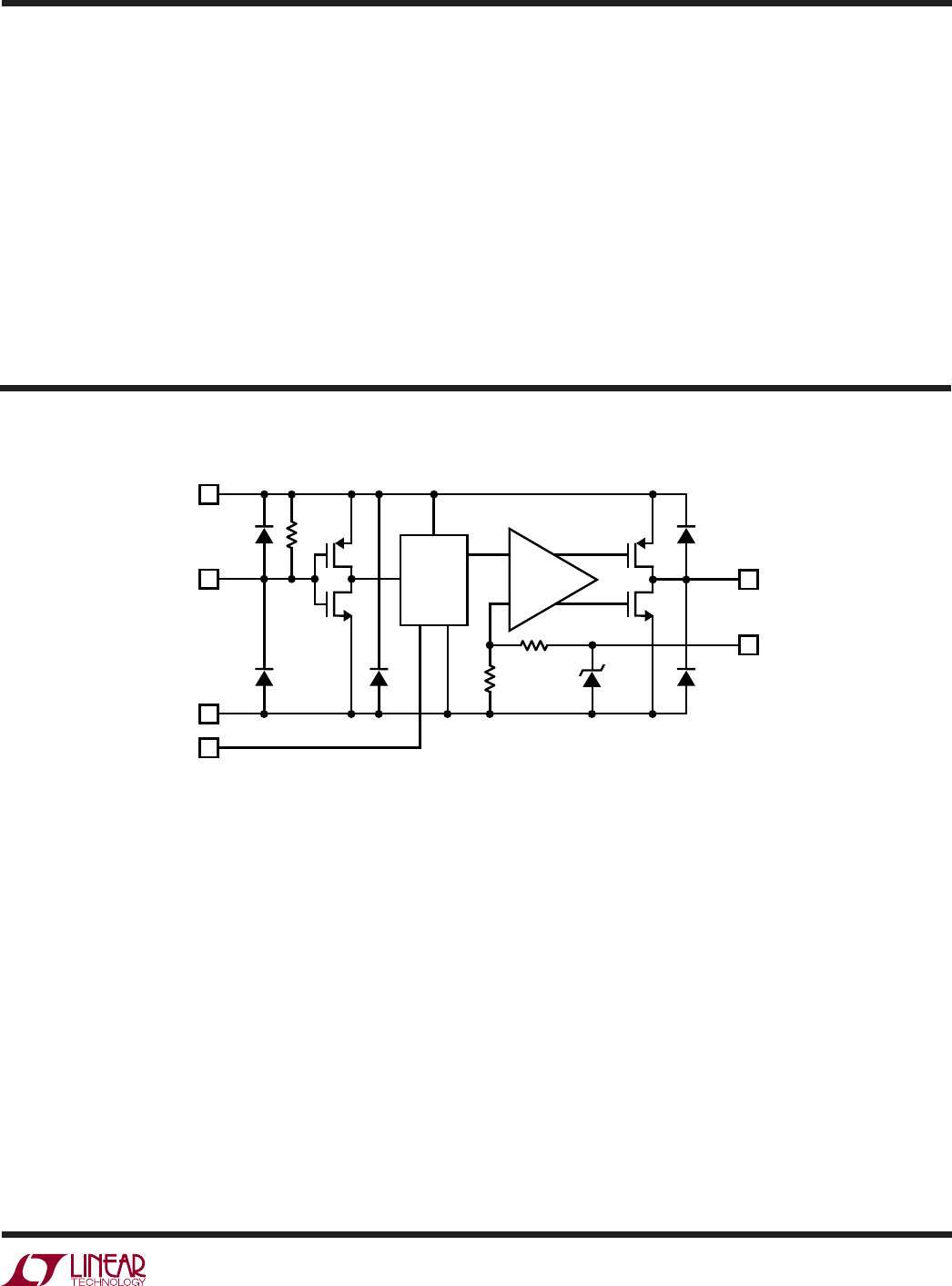
pin FuncTions
SHDN (Pin 1): Shutdown Input. This active low input
powers down the device to <20µA. If left open, an inter-
nal pull-up resistor puts the part in normal operation. It
is recommended to tie this pin high externally for best
performance during normal operation.
V
IN
(Pin 2): Power Supply. Bypass V
IN
with a 0.1µF, or
larger, capacitor to GND.
GND (Pin 4): Device Ground. This pin is the main ground
and must be connected to a noise-free ground plane.
V
OUT_S
(Pin 6): V
OUT
Sense Pin. Connect this pin at the
load and route with a wide metal trace to minimize load
regulation errors. This pin sinks 2mA. Output error is
R
TRACE
• 2mA, regardless of load current. For load currents
<100µA, tie directly to V
OUT_F
pin.
V
OUT_F
(Pin 7): V
OUT
Force Pin. This pin sources and
sinks current to the load. An output capacitor of 2.7µF to
100µF is required.
GND (Pins 3, 5, 8): Internal Function. Ground these
pins.
blocK DiagraM
–
+
V
OUT_F
7
2
V
OUT_S
6655 BD
6
BANDGAP
V
IN
1
4
SHDN
GND
GND
3,5,8