
Datasheet


LTC6903/LTC6904
6
69034fe
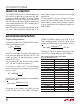
pin FuncTions
GND (Pin 1): Negative Power Supply (Ground). Should
be tied directly to a ground plane for best performance.
SDI (Pin 2): Serial Data Input. Data for serial transfer is
presented on this pin.
SCK (Pin 3): Serial Port Clock. Input, positive edge trig-
gered. Clocks serial data in on rising edge.
SEN (Pin 4): Serial Port Enable (LTC6903 Only). Input,
active LOW. Initiates serial transaction when brought LOW,
finalizes transaction when brought HIGH after 16 clocks.
ADR (Pin 4): Serial Port Address (LTC6904 Only). Sets
the I
2
C serial port address.
CLK (Pin 5): Auxiliary Clock Output. Frequency set by
serial port.
CLK (Pin 6): Main Clock Output. Frequency set by serial port.
OE (Pin 7): Asynchronous Output Enable. CLK and CLK
are set LOW when this pin is LOW.
V
+
(Pin 8): Positive Power Supply. This supply must be
kept free from noise and ripple. It should be bypassed
directly to a ground plane with a quality 0.1µF capacitor.
Additional bypass may be necessary for operation at high
frequency or under larger loads.
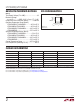
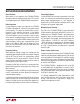
block DiagraM
21 3 4
67
5
8
–
+
MASTER
OSCILLATOR
f
MO
= 68MHz • kΩ
I
SET
V
+
– V
SET
PROGRAMMABLE
DIVIDER
+
–
I
SET
V
SET
A1
SERIAL PORT
V
+
OE
GND
DAC OCT
SDI SCK SEN (LTC6903)
ADR (LTC6904)
CLK CLK
69034 BD