
Datasheet


LTC6906
11
6906fc
APPLICATIONS INFORMATION
Alternative Methods for Setting the Output Frequency
Any means of sinking current from the SET pin will control
the output frequency of the LTC6906. Equation2 (repeated
below) gives the fundamental relationship between fre-
quency and the SET pin voltage and current:
t
OSC
=
1
ƒ
OSC
=
V
SET
I
SET
•10pF
(2)
This equation shows that the LTC6906 converts conduc-
tance (I
SET
/V
SET
) to frequency or, equivalently, converts
resistance (R
SET
= V
SET
/I
SET
) to period.
V
SET
is the voltage across an internal diode, and as such
it is given approximately by:
V
SET
≅ V
T
• Log
e
I
SET
I
S
≅ 25.9mV • Log
e
I
SET
82 • 10
–18
A
⎛
⎝
⎜
⎞
⎠
⎟
– 2.3mV/°C
where
V
T
= kT/q = 25.9mV at T = 300°K (27°C)
I
S
≅ 82 • 10
–18
Amps
(I
S
is also temperature dependent)
V
SET
varies with temperature and the SET pin current.
The response of V
SET
to temperature is shown in the
Typical Performance graphs. V
SET
changes approximately
–2.3mV/°C. At room temperature V
SET
increases 18mV/
octave or 60mV/decade of increase in I
SET
.
If the SET pin is driven with a current source generating
I
SET
, the oscillator output frequency will be:
ƒ
OSC
≅
I
SET
10pF
25.9mV • Cn
I
SET
82 • 10
–18
A
⎛
⎝
⎜
⎞
⎠
⎟
– 2.3mV/°C
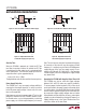
Figure 17 and Figure 18 show a current controlled oscil-
lator and a voltage controlled oscillator. These circuits are
not highly accurate if used alone, but can be very useful
if they are enclosed in an overall feedback circuit such as
a phase-locked loop.
Figure 17. Current Controlled Oscillator
Figure 18. Voltage Controlled Oscillator
Figure 16. Using the LTC6906 at Higher Supply Voltages
V
+
GND
DIV
OUT
GRD
SET
LTC6906
R
SET
100Ω
V
+
3.6V TO 5.5V DC
1μF
6906 F16
Jitter and Divide Ratio
At a given output frequency, a higher master oscillator
frequency and a higher divide ratio will result in lower
jitter and higher power supply dissipation. Indeterminate
jitter percentage will decrease by a factor of slightly less
than the square root of the divider ratio, while determinate
jitter will not be similarly attenuated. Please consult the
specification tables for typical jitter at various divider ratios.
V
+
GND
DIV
OUT
GRD
SET
LTC6906
I
CTRL
0.65μA TO 6.5μA
V
+
6906 F17
100kHz TO 1MHz
V
+
GND
DIV
OUT
GRD
SET
LTC6906
R
SET
100k
V
CTRL
0V TO 0.585V
V
+
6906 F18
1MHz TO 100kHz