
Datasheet


LTC6909
8
6909fa
I
RES
(µA)
V
RES
= V
+
– V
SET
1.4
1.3
1.2
1.1
1.0
0.9
0.8
0.1 10 100 1000
6909 F01
1
V
+
= 5V
V
+
= 3V
T
A
= 25°C
As shown in the Block Diagram, the LTC6909’s master
oscillator is controlled by the ratio of the voltage between
the V
+
A and SET pins and the current entering the SET pin
(I
MASTER
). When the spread spectrum frequency modula-
tion (SSFM) is disabled, I
MASTER
is strictly determined by
the (V
+
A – V
SET
) voltage and the R
SET
resistor. When SSFM
is enabled, I
MASTER
is modulated by a filtered pseudoran-
dom noise (PRN) signal. Here the I
MASTER
current is a
random value uniformly distributed between (I
SET
– 10%)
and (I
SET
+ 10%). In this way, the frequency is modulated
to produce an approximately flat frequency spectrum,
centered about the set frequency with a bandwidth equal
to approximately 20% of the center frequency.
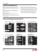
The voltage on the SET pin is forced to approximately 1.1V
below V
+
A by the PMOS transistor and its gate bias volt-
age. This voltage is accurate to ±5% at a particular input
current and supply voltage (see Figure 1). The LTC6909
is optimized for use with resistors between 20k and 400k
corresponding to master oscillator frequencies between
500kHz and 10MHz. Accurate master oscillator frequen-
cies up to 20MHz (R
SET
= 10k) are attainable if the supply
voltage is greater than 4V. The R
SET
resistor, connected
between the V
+
A and SET pins, locks together the (V
+
A –
V
SET
) voltage and the current I
SET
. This allows the parts
to attain excellent frequency accuracy regardless of the
precision of the SET pin. The master oscillation frequency is:
f
MASTER
= 20MHz • 10k/R
SET
Figure 1. V
+
– V
SET
Variation with I
RES
When the spread spectrum frequency modulation (SSFM)
is disabled, the master oscillator frequency is stationary.
When SSFM is enabled, the master oscillator frequency
varies from 0.9 • f
MASTER
to 1.1 • f
MASTER
.
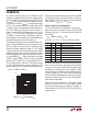
Output Frequency and Configurations
The output frequency of the LTC6909 is set by the R
SET
resistor value and the connections of the PH0, PH1 and
PH2 logic input pins. The following formula defines the
relationship:
f
OUT
= 20MHz • 10k/(R
SET
• PH)
where PH = 3, 4, 5, 6, 7 or 8 and is defined as follows:
PH2 PH1 PH0 MODE
0 0 0 All Outputs Are Floating (Hi-Z)
0 0 1 All Outputs Are Held Low
0 1 0 3-Phase Mode (PH = 3)
0 1 1 4-Phase Mode (PH = 4)
1 0 0 5-Phase Mode (PH = 5)
1 0 1 6-Phase Mode (PH = 6)
1 1 0 7-Phase Mode (PH = 7)
1 1 1 8-Phase Mode (PH = 8)
The PH0, PH1 and PH2 pins are standard logic input pins.
These pins do not have any active pull-up or pull-down
circuitry. As such, they cannot be left floating and must be
connected to a valid logic high or low voltage. The PH0,
PH1 and PH2 pin connections not only divide the master
oscillator frequency by the value PH but also determine
the phase relationship between the output signals. Figure
2 shows the output waveforms for each of the eight pos-
sible output configurations.
Note that 2-phase, complementary (180° phase shifted)
outputs are available in the 4-, 6- and 8-phase modes
by choosing the correct pair of signals. For example, in
4-phase mode, OUT1 and OUT3 (or OUT2 and OUT4) are
complementary.
operAtion