
Datasheet


4
LTC690/LTC691
LTC694/LTC695
E
LECTR
IC
AL C CHARA TERIST
ICS
The ● denotes specifications which apply over the operating temperature
range, otherwise specifications are at T
A
= 25°C. V
CC
= full operating range, V
BATT
= 2.8V, unless otherwise noted.
PARAMETER CONDITONS MIN TYP MAX UNITS
RESET, RESET, WDO, LOW LINE Output Source Current 1 3 25 µA
Output Short-Circuit Current (Note 4)
Output Sink Current 25 mA
WDI Input Threshold Logic Low 0.8 V
Logic High 3.5
WDI Input Current WDI = V
OUT
● 450µA
WDI = 0V
● –50 –8
Power-Fail Detector
PFI Input Threshold V
CC
= 5V ● 1.25 1.3 1.35 V
PFI Input Threshold PSRR 0.3 mV/V
PFI Input Current ±0.01 ±25 nA
PFO Output Voltage (Note 4) I
SINK
= 3.2mA 0.4 V
I
SOURCE
= 1µA 3.5
PFO Short-Circuit Source Current (Note 4) PFI = HIGH, PFO = 0V 1 3 25 µA
PFI = LOW, PFO = V
OUT
25 mA
PFI Comparator Response Time (Falling) ∆V
IN
= –20mV, V
OD
= 15mV 2 µs
PFI Comparator Response Time (Rising) (Note 4) ∆V
IN
= 20mV, V
OD
= 15mV 40 µs
with 10kΩ Pull-Up 8
Chip Enable Gating
CE IN Threshold V
IL
0.8 V
V
IH
2.0
CE IN Pull-Up Current (Note 7) 3 µA
CE OUT Output Voltage I
SINK
= 3.2mA 0.4 V
I
SOURCE
= 3.0mA V
OUT
– 1.50
I
SOURCE
= 1µA, V
CC
= 0V V
OUT
– 0.05
CE Propagation Delay V
CC
= 5V, C
L
= 20pF 20 35 ns
● 20 45
CE OUT Output Short-Circuit Current Output Source Current 30 mA
Output Sink Current 35
Oscillator
OSC IN Input Current (Note 7) ±2 µA
OSC SEL Input Pull-Up Current (Note 7) 5 µA
OSC IN Frequency Range OSC SEL = 0V ● 0 250 kHz
OSC IN Frequency with External Capacitor OSC SEL = 0V, C
OSC
= 47pF 4 kHz
Note 1: Absolute Maximum Ratings are those values beyond which the life
of device may be impaired.
Note 2: All voltage values are with respect to GND.
Note 3: For military temperature range parts or for the LTC692 and
LTC693, consult the factory.
Note 4: The output pins of BATT ON, LOW LINE, PFO, WDO, RESET and
RESET have weak internal pull-ups of typically 3µA. However, external
pull-up resistors may be used when higher speed is required.
Note 5: The LTC690 and LTC691 have minimum reset active time of 35ms
(50ms typically) while the LTC694 and LTC695 have longer minimum
reset active time of 140ms (200ms typically). The reset active time of the
LTC691 and LTC695 can be adjusted (see Table 2 in Applications
Information section).
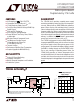
Note 6: The external clock feeding into the circuit passes through the
oscillator before clocking the watchdog timer (See Block Diagram).
Variation in the time-out period is caused by phase errors which occur
when the oscillator divides the external clock by 64. The resulting variation
in the time-out period is 64 clocks plus one clock of jitter.
Note 7: The input pins of CE IN, OSC IN and OSC SEL have weak internal
pullups which pull to the supply when the input pins are floating.