
Datasheet

LTC6912
21
6912fa
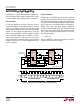
APPLICATIO S I FOR ATIO
WUUU
Offset Voltage vs Gain Setting
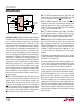
The electrical tables list DC offset (error), V
OS(OA)
, at the
inputs of the internal op amp (See Figure 1). The electrical
tables also show the resulting, gain dependent offset
voltage referred to the INA, or INB pins, V
OS(IN)
. The two
measures are related through the feedback/input resistor
ratio, which equals the nominal gain-magnitude setting,
|GAIN|:
V
OS(IN)
= (1 + 1/|GAIN|) V
OS(OA)
Offset voltages at any gain setting can be inferred from this
relationship. For example, an internal amplifier offset
V
OS(OA)
of 1mV will appear referred to the INA, INB pins as
2mV at a gain setting of 1, or 1.5mV at a gain setting of 2.
At high gains, V
OS(IN)
approaches V
OS(OA)
. (Offset voltage
is random and can have either polarity centered on 0V).
The MOS input circuitry of the internal op amp in Figure 1
draws negligible input currents (less than 10µA), so only
V
OS(OA)
and the GAIN affect the overall amplifier’s offset.
AC-Coupled Operation
Adding capacitors in series with the INA and INB pins
converts the LTC6912-X into a dual AC-coupled inverting
amplifier, suppressing the input signal’s DC level (and also
adding the additional benefit of reducing the offset voltage
from the LTC6912-X’s amplifier itself). No further compo-
nents are required because the input of the LTC6912-X
biases itself correctly when a series capacitor is added.
The INA and INB analog input pins connect internally to a
resistor whose nominal value varies between 10kΩ and
1kΩ depending on the version of LTC6912 used (see the
rightmost column of Tables 1 and 2). Therefore, the low
frequency cutoff will vary with capacitor and gain setting.
If, for example, a low frequency corner of 1kHz (or lower)
on the LTC6912-1 is desired, use a series capacitor of
0.16µF or larger. 0.16µF has a reactance of 1kΩ at 1kHz,
giving a 1kHz lower –3dB frequency for gain settings of
10V/V through 100V/V. If the LTC6912-1 is operated at
lower gain settings with a 0.16µF capacitor, the higher
input resistance will reduce the lower corner frequency
down to 100Hz at a gain setting of 1V/V. These frequencies
scale inversely with the value of input capacitor used.
Note that operating the LTC6912 family in “zero” gain
mode (digital state 0000) open circuits both the INA and
INB pins and this demands some care if employed with a
series AC coupling input capacitor. When the chip enters
the zero gain mode, the opened INA or INB pin tends to
sample and freeze the voltage across the capacitor to the
value it held just before the zero gain state. This can place
the INA or INB pin at or near the DC potential of a supply
rail. (The INA or INB pin may also drift to a supply potential
in this state due to small leakage currents.) To prevent
driving the INA or INB pin outside the supply limit and
potentially damaging the chip, avoid AC input signals in
the zero gain state with an AC coupling capacitor. Also,
switching later to a non-zero gain value will cause a
transient pulse at the output of the LTC6912-1 (with a time
constant set by the capacitor value and the new LTC6912-1
input resistance value). This occurs because the INA and
INB pins return to the AGND potential forcing transient
current sourced by the amplifier output to charge the AC
coupling capacitor to its proper DC blocking value.
SNR and Dynamic Range
The term “dynamic range” is much used (and abused)
with signal paths. Signal-to-noise (SNR) is an unambigu-
ous comparison of signal and noise levels, measured in
the same way and under the same operating conditions. In
a variable gain amplifier, however, further characterization
is useful because both noise and maximum signal level in
the amplifier will vary with the gain setting, in general. In
the LTC6912-X, maximum output signal is independent of
gain (and is near the full power supply voltage, as detailed
in the swing sections of the Electrical Characteristics
table). The maximum input level falls with increasing gain,
and the input-referred noise falls as well (listed also in the
table). To summarize the useful signal range in such an
amplifier, we define dynamic range (DR) as the ratio of
maximum input (at unity gain) to minimum input-referred
noise (at maximum gain). This DR has a physical interpre-
tation as the range of signal levels that will experience an
SNR above unity V/V or 0dB. At a 10V total power supply,
DR in the LTC6912-X (gains 0V/V to 100V/V), the DR is
typically 115dB (the ratio of 9.9 V
P-P
, or 3.5V
RMS
, maxi-
mum input to the 6.3µV
RMS
high gain input noise). The