
Datasheet

LTC6993-1/LTC6993-2
LTC6993-3/LTC6993-4
12
69931234fb
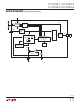
OPERATION
The LTC6993 is built around a master oscillator with a 1µs
minimum period. The oscillator is controlled by the SET
pin current (I
SET
) and voltage (V
SET
), with a 1µs/50kΩ
conversion factor that is accurate to ±1.7% under typical
conditions.
t
MASTER
=
1µs
50kΩ
•
V
SET
I
SET
A feedback loop maintains V
SET
at 1V ±30mV, leaving
I
SET
as the primary means of controlling the pulse width.
The simplest way to generate I
SET
is to connect a resistor
(R
SET
) between SET and GND, such that I
SET
= V
SET
/R
SET
.
The master oscillator equation reduces to:
t
MASTER
= 1µs •
R
SET
50kΩ
From this equation, it is clear that V
SET
drift will not affect
the pulse width when using a single program resistor
(R
SET
). Error sources are limited to R
SET
tolerance and
the inherent pulse width accuracy ∆t
OUT
of the LTC6993.
R
SET
may range from 50k to 800k (equivalent to I
SET
between 1.25µA and 20µA).
A trigger signal (rising or falling edge on TRIG pin
) latches
the output to the active state, beginning the output pulse. At
the same time, the master oscillator is enabled to time the
duration of the output pulse. When the desired pulse width
is reached, the master oscillator resets the output latch.
The LTC6993 also includes a programmable frequency
divider which can further divide the frequency by 1, 8, 64,
512, 4096, 2
15
, 2
18
or 2
21
. This extends the pulse width
duration by those same factors. The divider ratio N
DIV
is
set by a resistor divider attached to the DIV pin.
t
OUT
=
N
DIV
50kΩ
•
V
SET
I
SET
• 1µs
With R
SET
in place of V
SET
/I
SET
the equation reduces to:
t
OUT
=
N
DIV
• R
SET
50kΩ
• 1µs
DIVCODE
The DIV pin connects to an internal, V
+
referenced 4-bit A/D
converter that determines the DIVCODE value. DIVCODE
programs two settings on the LTC6993:
1. DIVCODE determines the frequency divider setting,
N
DIV
.
2. DIVCODE determines the polarity of OUT pin, via the
POL bit.
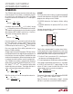
V
DIV
may be generated by a resistor divider between V
+
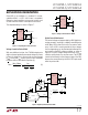
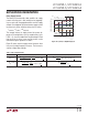
and GND as shown in Figure 1.
Figure 1. Simple Technique for Setting DIVCODE
69931234 F01
LTC6993
V
+
DIV
GND
R1
R2
2.25V TO 5.5V
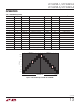
Table 1 offers recommended 1% resistor values that ac-
curately produce the correct voltage division as well as the
corresponding N
DIV
and POL values for the recommended
resistor pairs. Other values may be used as long as:
1. The V
DIV
/V
+
ratio is accurate to ±1.5% (including resis-
tor tolerances and temperature effects).
2. The driving impedance (R1||R2) does not exceed 500kΩ.
If the voltage is generated by other means (i.e., the output
of a DAC) it must track the V
+
supply voltage. The last
column in Table 1 shows the ideal ratio of V
DIV
to the
supply voltage, which can also be calculated as:
V
DIV
V
+
=
DIVCODE+ 0.5
16
± 1.5%
For example, if the supply is 3.3V and the desired DIVCODE
is 4, V
DIV
= 0.281 • 3.3V = 928mV ± 50mV.
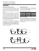
Figure 2 illustrates the information in Table 1, showing
that N
DIV
is symmetric around the DIVCODE midpoint.