
Datasheet

LTC6993-1/LTC6993-2
LTC6993-3/LTC6993-4
16
69931234fb
APPLICATIONS INFORMATION
Basic Operation
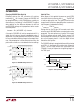
The simplest and most accurate method to program
the LTC6993 is to use a single resistor, R
SET
, between
the SET and GND pins. The design procedure is a four
step process. Alternatively, Linear Technology offers the
easy-to-use TimerBlox Designer tool to quickly design
any LTC6993 based circuit. Download the free TimerBlox
Designer software at www.linear.com/timerblox.
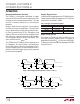
Step 1: Select the POL Bit Setting.
The LTC6993 can generate positive or negative output
pulses, depending on the setting of the POL bit
. The POL
bit is the DIVCODE MSB, so any DIVCODE ≥ 8 has POL
= 1
and produces active-low pulses.
Step 2: Select LTC6993 Version.
Tw o input-related choices dictate the proper LTC6993 for
a given application:
• Is TRIG a rising or falling-edge input?
• Should retriggering be allowed?
Use Table 2 to select a particular variety of LTC6993.
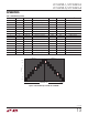
Step 3: Select the N
DIV
Frequency Divider Value.
As explained earlier, the voltage on the DIV pin sets the
DIVCODE which determines both the POL bit and the N
DIV
value. For a given output pulse width (t
OUT
), N
DIV
should
be selected to be within the following range:
t
OUT
16µs
≤N
DIV
≤
t
OUT
1µs
(1)
To minimize supply current, choose the lowest N
DIV
value.
However, in some cases a higher value for N
DIV
will provide
better accuracy (see Electrical Characteristics).
Table 1 can also be used to select the appropriate N
DIV
values for the desired t
OUT
.
With POL already chosen, this completes the selection of
DIVCODE. Use Table 1 to select the proper resistor divider
or V
DIV
/V
+
ratio to apply to the DIV pin.
Step 4: Calculate and Select R
SET
.
The final step is to calculate the correct value for R
SET
using the following equation:
R
SET
=
50k
1µs
•
t
OUT
N
DIV
(2)
Select the standard resistor value closest to the calculated
value.
Example: Design a one-shot circuit that satisfies the fol-
lowing requirements:
• t
OUT
= 100µs
• Negative Output Pulse
• Rising-Edge Trigger Input
• Retriggerable Input
• Minimum power consumption
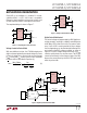
Step 1: Select the POL Bit Setting.
For inverted (negative) output pulse, choose POL = 1.
Step 2: Select the LTC6993 Version.
A rising-edge retriggerable input requires the LTC6993
-2.
Step 3: Select the N
DIV
Frequency Divider Value.
Choose an N
DIV
value that meets the requirements of
Equation (1), using t
OUT
= 100µs:
6.25 ≤ N
DIV
≤ 100
Potential settings for N
DIV
include 8 and 64. N
DIV
= 8 is
the best choice, as it minimizes supply current by us-
ing a large R
SET
resistor. POL = 1 and N
DIV
= 8 requires
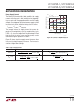
DIVCODE = 14. Using Table 1, choose R1 = 102k and
R2 = 976k values to program DIVCODE = 14.
Step 4: Select R
SET
.
Calculate the correct value for R
SET
using Equation (2):
R
SET
=
50k
1µs
•
100µs
8
= 625k