
Datasheet


LTC6993-1/LTC6993-2
LTC6993-3/LTC6993-4
10
69931234fb
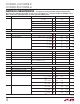
PIN FUNCTIONS
(DCB/S6)
V
+
(Pin 1/Pin 5): Supply Voltage (2.25V to 5.5V). This sup-
ply should be kept free from noise and ripple. It should be
bypassed directly to the GND pin with a 0.1µF capacitor.
DIV (Pin 2/Pin 4): Programmable Divider and Polarity
Input. The DIV pin voltage (V
DIV
) is internally converted
into a 4-bit result (DIVCODE). V
DIV
may be generated by
a resistor
divider between V
+
and GND. Use 1% resistors
to ensure an accurate result. The DIV pin and resistors
should be shielded from the OUT pin or any other traces
that have fast edges. Limit the capacitance on the DIV pin
to less than 100pF so that V
DIV
settles quickly. The MSB of
DIVCODE (POL) determines the polarity of the OUT pins.
When POL = 0 the output produces a
positive pulse. When
POL = 1 the output produces a negative pulse.
SET (Pin 3/Pin 3): Pulse Width Setting Input. The voltage
on the SET pin (V
SET
) is regulated to 1V above GND. The
amount of current sourced from the SET pin (I
SET
) pro-
grams the master oscillator frequency. The I
SET
current
range is 1.25µA to 20µA. The output pulse will continue
indefinitely if I
SET
drops below approximately 500nA,
and will terminate when I
SET
increases again. A resistor
connected between SET and GND is the most accurate
way to set the pulse width. For best performance, use
a precision metal or thin film resistor of 0.5% or better
tolerance and 50ppm/°C or better temperature coefficient.
For lower accuracy applications an inexpensive 1% thick
film resistor may be used.
Limit the capacitance on the SET pin to less than 10pF
to minimize jitter and ensure stability. Capacitance less
than 100pF maintains the stability of the feedback circuit
regulating the V
SET
voltage.
TRIG (Pin 4/Pin 1): Trigger Input. Depending on the ver-
sion, a rising or falling edge on TRIG will initiate the output
pulse. LTC6993-1 and LTC6993-2 are rising-edge sensi-
tive. LTC6993-3 and LTC6993-4 are falling-edge sensitive.
The LTC6993
-2 and LTC6993-4 are retriggerable, allowing
the pulse width to be extended by additional trigger signals
that occur while the output is active. The LTC6993
-1/
LTC6993-3 will ignore additional trigger inputs until the
output pulse has terminated.
GND (Pin 5/Pin 2): Ground. Tie to a low inductance ground
plane for best performance.
OUT (Pin 6/Pin 6): Output. The OUT pin swings from
GND to V
+
with an output resistance of approximately
30Ω. When driving an LED or other low impedance load
a series output resistor should be used to limit source/
sink current
to 20mA.
69931234 PF
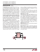
LTC6993
TRIG
GND
SET
OUT
V
+
DIV
C1
0.1µF
R
SET
R2
R1
V
+
V
+