
Datasheet


LTC6993-1/LTC6993-2
LTC6993-3/LTC6993-4
20
69931234fb
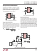
Supply Bypassing and PCB Layout Guidelines
The LTC6993 is an accurate monostable multivibrator when
used in the appropriate manner. The part is simple to use
and by following a few rules, the expected performance is
easily achieved. Adequate supply bypassing and proper
PCB layout are important to ensure this.
Figure 13 shows example PCB layouts for both the SOT-23
and DCB packages using 0603 sized passive components.
The layouts
assume a two layer board with a ground plane
layer beneath and around the LTC6993. These layouts are
a guide and need not be followed exactly.
1. Connect the bypass capacitor, C1, directly to the V
+
and
GND pins using a low inductance path. The connection
from C1 to the V
+
pin is easily done directly on the top
layer. For the DCB package, C1’s connection to GND is
also simply done on the top layer. For the SOT-23, OUT
can be routed through the C1 pads to allow a good C1
GND connection. If the PCB design rules do not allow
that, C1’s GND connection can be accomplished through
multiple vias to the ground plane. Multiple vias for both
the GND pin connection to the ground plane and the
C1 connection to the ground plane are recommended
to minimize the inductance. Capacitor C1 should be a
0.1µF ceramic capacitor.
2. Place all passive components on the top side of the
board. This minimizes trace inductance.
3. Place R
SET
as close as possible to the SET pin and
make a direct, short connection. The SET pin is a cur-
rent summing node and currents injected into this pin
directly modulate the output pulse width. Having a short
connection minimizes the exposure to signal pickup.
4. Connect R
SET
directly to the GND pin. Using a long path
or vias to the ground plane will not have a significant
affect on accuracy, but a direct, short connection is
recommended and easy to apply.
5. Use a ground trace to shield the SET pin. This provides
another layer of protection from radiated signals.
6. Place R1 and R2 close to the DIV pin. A direct, short
connection to the DIV pin minimizes the external signal
coupling.
69931234 F13
LTC6993
TRIG
GND
SET
OUT
V
+
DIV
C1
0.1µF
R1
R2
R
SET
V
+
V
+
DIV
SET
OUT
GND
TRIG
C1R1
R2
V
+
R
SET
DCB PACKAGE
TRIG
GND
SET
OUT
V
+
DIV
R2
V
+
R
SET
TSOT-23 PACKAGE
R1
C1
Figure 13. Supply Bypassing and PCB Layout
APPLICATIONS INFORMATION