
Datasheet
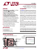
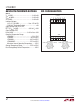


LTM2881
6
2881fg
For more information www.linear.com/LTM2881
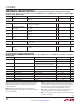
ISOLATION CHARACTERISTICS
T
A
= 25°C, LTM2881-3 V
CC
= 3.3V, LTM2881-5 V
CC
= 5.0V, V
L
= 3.3V unless
otherwise noted.
SYMBOL PARAMETER CONDITIONS MIN TYP MAX UNITS
V
ISO
Rated Dielectric Insulation Voltage 1 Minute (Derived from 1 Second Test) 2500 V
RMS
1 Second (Notes 5, 6) ±4400 V
DC
Common Mode Transient Immunity LTM2881-3 V
CC
= 3.3V, LTM2881-5 V
CC
= 5V,
V
L
= ON = 3.3V, V
CM
= 1kV, ∆t = 33ns (Note 2)
±30 kV/µs
V
IORM
Maximum Working Insulation Voltage (Notes 2, 5) 560
400
V
PEAK
V
RMS
Partial Discharge V
PR
= 1050 V
PEAK
(Note 2) 5 pC
CTI Comparative Tracking Index IEC 60112 (Note 2) 600 V
RMS
Depth of Erosion IEC 60112 (Note 2) 0.017 mm
DTI Distance Through Insulation (Note 2) 0.06 mm
Input to Output Resistance (Notes 2, 5) 10
9
Ω
Input to Output Capacitance (Notes 2, 5) 6 pF
Creepage Distance (Notes 2, 5) 9.48 mm
Note 1: Stresses beyond those listed under Absolute Maximum Ratings
may cause permanent damage to the device. Exposure to any Absolute
Maximum Rating condition for extended periods may affect device
reliability and lifetime.
Note 2: Guaranteed by design and not subject to production test.
Note 3: Maximum Data rate is guaranteed by other measured parameters
and is not tested directly.
Note 4: This µModule transceiver includes overtemperature protection that
is intended to protect the device during momentary overload conditions.
Junction temperature will exceed 125°C when overtemperature protection
is active. Continuous operation above specified maximum operating
junction temperature may result in device degradation or failure.
Note 5: Device considered a 2-terminal device. Pin group A1 through B8
shorted together and pin group K1 through L8 shorted together.
Note 6: The rated dielectric insulation voltage should not be interpreted as
a continuous voltage rating.
SYMBOL PARAMETER CONDITIONS MIN TYP MAX UNITS
t
ZLD
, t
ZHD
,
t
LZD
, t
HZD
Driver Output Enable or Disable
Time
R
L
= 500Ω, C
L
= 50pF
(Figure 5)
l
400 ns
Receiver
t
PLHR
t
PHLR
Receiver Input to Output C
L
= 15pF, V
CM
= 2.5V, |V
AB
| = 1.4V,
t
R
and t
F
< 4ns, (Figure 6)
l
100 140 ns
t
SKEWR
Differential Receiver Skew
|t
PLHR
- t
PHLR
|
C
L
= 15pF
(Figure 6)
l
1 8 ns
t
RR
t
FR
Receiver Output Rise or Fall Time C
L
= 15pF
(Figure 6)
l
3 12.5 ns
t
ZLR
, t
ZHR
,
t
LZR
, t
HZR
Receiver Output Enable Time R
L
=1kΩ, C
L
= 15pF
(Figure 7)
l
50 ns
t
RTEN
, t
RTZ
Termination Enable or Disable
Time
RE = 0V, DE = 0V, V
AB
= 2V, V
B
= 0V (Figure 8)
l
100 µs
Generic Logic Input
t
PLHL1
t
PHLL1
D
IN
to D
OUT
Input to Output C
L
= 15pF,
t
R
and t
F
< 4ns
l
60 100 ns
Power Supply Generator
V
CC2
–GND2 Supply Start-Up
Time
(0V to 4.5V)
ON
V
L
, No Load
l
325 800 µs
SWITCHING CHARACTERISTICS
The l denotes the specifications which apply over the full operating
temperature range, otherwise specifications are at T
A
= 25°C. LTM2881-3 V
CC
= 3.3V, LTM2881-5 V
CC
= 5.0V, V
L
= 3.3V, GND = GND2 =
0V, ON = V
L
unless otherwise noted.