
Datasheet
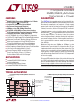


LTM2881
9
2881fg
For more information www.linear.com/LTM2881
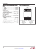
LOGIC SIDE (V
CC
, V
L
, GND)
D
OUT
(Pin A1): General Purpose Logic Output. Logic
output connected through isolation path to D
IN
. Under
the condition of an isolation communication failure D
OUT
is in a high impedance state.
TE (Pin A2): Terminator Enable. A logic high enables a
termination resistor (typically 120Ω) between pins A and B.
DI (Pin A3): Driver Input. If the driver outputs are enabled
(DE high), then a low on DI forces the driver noninverting
output (Y) low and the inverting output (Z) high. A high
on DI, with the driver outputs enabled, forces the driver
noninverting output (Y) high and inverting output (Z) low.
DE (Pin A4): Driver Enable. A logic low disables the driver
leaving the outputs Y and Z in a high impedance state. A
logic high enables the driver.
RE (Pin A5): Receiver Enable. A logic low enables the
receiver output. A logic high disables RO to a high imped
-
ance state.
RO (Pin A6):
Receiver Output. If the receiver output is
ena
bled (RE low) and if A – B is > 200mV, RO is a logic
high, if A – B is < –200mV RO is a logic low. If the receiver
inputs are open, shorted, or terminated without a valid
signal, RO will be high. Under the condition of an isolation
communication failure RO is in a high impedance state.
V
L
(Pin A7): Logic Supply. Interface supply voltage for
pins RO, RE, TE, DI, DE, D
OUT
, and ON. Recommended
operating voltage is 1.62V to 5.5V. Internally bypassed
to GND with 2.2µF.
ON (Pin A8): Enable. Enables power and data communica
-
tion through the isolation barrier. If ON is high the part is
enabled and power and communications are functional
to the isolated side. If ON is low the logic side is held in
reset and the isolated side is unpowered.
GND (Pins B1-B5): Cir
cuit Ground.
V
CC
(Pins B6-B8): Supply Voltage. Recommended operat-
ing voltage is 3V to 3.6V for LTM2881-3 and 4.5V to 5.5V
for LTM2881-5. Internally bypassed to GND with 2.2µF
.
PIN FUNCTIONS
ISOLATED SIDE (V
CC2
, GND2)
D
IN
(Pin L1): General Purpose Isolated Logic Input. Logic
input on the isolated side relative to V
CC2
and GND2. A
logic high on D
IN
will generate a logic high on D
OUT
. A
logic low on D
IN
will generate a logic low on D
OUT
.
SLO (Pin L2): Driver Slew Rate Control. A low input, rela-
tive to GND2, will force the driver into a reduced slew rate
mode for reduced EMI. A high input, relative to GND2,
puts the driver into full speed mode to support maximum
data rates.
Y (Pin
L3):
Non Inverting Driver Output. High impedance
when the driver is disabled.
Z (Pin L4): Inverting Driver Output. High impedance when
the driver is disabled.
B (Pin L5): Inverting Receiver Input. Impedance is > 96kΩ
in receive mode with TE low or unpowered.
A (Pin L6): Non Inverting Receiver Input. Impedance is
> 96kΩ in receive mode with TE low or unpowered.
V
CC2
(Pins L7-L8): Isolated Supply Voltage. Internally
generated from V
CC
by an isolated DC/DC converter and
regulated to 5V. Internally bypassed to GND2 with 2.2µF.
GND2 (Pins K1-K8): Isolated Side Circuit Ground. The
pads should be connected to the isolated ground and/or
cable shield.