
Datasheet

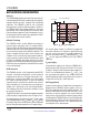


LTM2882
14
2882fe
For more information www.linear.com/LTM2882
applicaTions inForMaTion
PCB Layout
The high integration of the LTM2882 makes PCB layout
very simple. However, to optimize its electrical isolation
characteristics, EMI, and thermal performance, some
layout considerations are necessary.
• Under heavily loaded conditions V
CC
and GND current
can exceed 300mA. Sufficient copper must be used
on the PCB to insure resistive losses do not cause the
supply voltage to drop below the minimum allowed
level. Similarly, the V
CC2
and GND2 conductors must
be sized to support any external load current. These
heavy copper traces will also help to reduce thermal
stress and improve the thermal conductivity.
• Input and Output decoupling is not required, since these
components are integrated within the package. An ad
-
ditional bulk capacitor with a value of 6.8µF to 22µF is
recommended. The high ESR of this capacitor reduces
board resonances and minimizes voltage spikes caused
by hot plugging of the supply voltage. For EMI sensitive
applications, an additional low ESL ceramic capacitor of
1µF to 4.7µF, placed as close to the power and ground
terminals as possible, is recommended. Alternatively, a
number of smaller value parallel capacitors may be used
to reduce ESL and achieve the same net capacitance.
• Do not
place copper on the PCB between the inner col-
umns of pads. This area must remain open to withstand
the rated isolation voltage.
• The
use of solid ground planes for GND and GND2
is recommended for non-EMI critical applications to
optimize signal fidelity, thermal performance, and to
minimize RF emissions due to uncoupled PCB trace
conduction. The drawback of using ground planes,
where EMI is of concern, is the creation of a dipole
antenna structure which can radiate differential voltages
formed between GND and GND2. If ground planes are
used it is recommended to minimize their area, and
use contiguous planes as any openings or splits can
exacerbate RF emissions.
• For large ground planes a small capacitance (≤ 330pF)
from GND to GND2, either discrete or embedded within
the substrate, provides a low impedance current return
path for the module parasitic capacitance, minimizing
any high frequency differential voltages and substantially
reducing radiated emissions. Discrete capacitance will
not be as effective due to parasitic ESL. In addition, volt
-
age rating
, leakage, and clearance must be considered
for
component selection. Embedding the capacitance
within the PCB substrate provides a near ideal capacitor
and eliminates component selection issues; however,
the PCB must
be 4 layers. Care
must be exercised in
applying either technique to insure the voltage rating
of the barrier is not compromised.
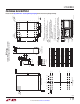
The PCB layout in Figures 7a to 7e show the low EMI
demo board for the LTM2882. The demo board uses a
combination of EMI mitigation techniques, including both
embedded PCB bridge capacitance and discrete GND to
GND2 capacitors. Tw o safety rated type Y2 capacitors
are used in series, manufactured by Murata, part number
GA342QR7GF471KW01L. The embedded capacitor ef
-
fectively suppresses
emissions above 400MHz, whereas
the discrete capacitors are more effective below 400MHz.
EMI performance is shown in Figure 8, measured using
a Gigahertz Transverse Electromagnetic (GTEM) cell and
method detailed in IEC 61000-4-20, “Testing and Mea
-
surement T
echniques – Emission and Immunity Testing
in T
ransverse Electromagnetic Waveguides.”