
Datasheet


LTM4622
7
Rev. G
For more information www.analog.com
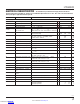
PIN FUNCTIONS
V
IN1
(D3, E2), V
IN2
(A2, B3): Power Input Pins. Apply input
voltage between these pins and GND pins. Recommend
placing input decoupling capacitance directly between
BOTH V
IN1
and V
IN2
pins and GND pins. Please note
the module internal control circuity is running off V
IN1
.
Channel 2 will not work without a voltage higher that 3.6V
present at V
IN1
.
GND (C1 to C2, B5, D5): Power Ground Pins for Both
Input and Output Returns.
INTV
CC
(C3): Internal 3.3V Regulator Output. The internal
power drivers and control circuits are powered from this
voltage. This pin is internally decoupled to GND with a
2.2µF low ESR ceramic capacitor. No additional external
decoupling capacitor needed.
SYNC/MODE (C5): Mode Select and External
Synchronization Input. Tie this pin to ground to force
continuous synchronous operation at all output loads.
Floating this pin or tying it to INTV
CC
enables high effi-
ciency Burst Mode operation at light loads. Drive this
pin with a clock to synchronize the LTM4622 switching
frequency. An internal phase-locked loop will force the
bottom power NMOS’s turn on signal to be synchronized
with the rising edge of the clock signal. When this pin is
driven with a clock, forced continuous mode is automati-
cally selected.
V
OUT1
(D1, E1), V
OUT2
(A1, B1): Power Output Pins
of Each Switching Mode Regulator. Apply output load
between these pins and GND pins. Recommend placing
output decoupling capacitance directly between these
pins and GND pins.
FREQ (C4): Frequency is set internally to 1MHz. An exter-
nal resistor can be placed from this pin to GND to increase
frequency, or from this pin to INTV
CC
to reduce frequency.
See the Applications Information section for frequency
adjustment.
RUN1 (D2), RUN2 (B2): Run Control Input of Each
Switching Mode Regulator Channel. Enables chip opera-
tion by tying RUN above 1.27V. Tying this pin below 1V
shuts down the specific regulator channel. Do not float
this pin.
PGOOD1 (D4), PGOOD2 (B4): Output Power Good with
Open-Drain Logic of Each Switching Mode Regulator
Channel. PGOOD is pulled to ground when the voltage
on the FB pin is not within ±8% (typical) of the internal
0.6V reference.
TRACK/SS1 (E3), TRACK/SS2 (A3): Output Tracking and
Soft-Start Pin of Each Switching Mode Regulator Channel.
It allows the user to control the rise time of the output
voltage. Putting a voltage below 0.6V on this pin bypasses
the internal reference input to the error amplifier, instead
it servos the FB pin to the TRACK voltage. Above 0.6V,
the tracking function stops and the internal reference
resumes control of the error amplifier. There’s an internal
1.4µA pull-up current from INTV
CC
on this pin, so putting
a capacitor here provides soft-start function. A default
internal soft-start ramp forces a minimum soft-start time
of 400µs.
FB1 (E4), FB2 (A4): The Negative Input of the Error
Amplifier for Each Switching Mode Regulator Channel.
Internally, this pin is connected to V
OUT
with a 60.4k preci-
sion resistor. Different output voltages can be programmed
with an additional resistor between FB and GND pins. In
PolyPhase
®
operation, tying the FB pins together allows
for parallel operation. See the Applications Information
section for details.
COMP1 (E5), COMP2 (A5): Current Control Threshold and
Error Amplifier Compensation Point of Each Switching
Mode Regulator Channel. The current comparator’s trip
threshold is linearly proportional to this voltage, whose
normal range is from 0.3V to 1.8V. Tie the COMP pins
together for parallel operation. The device is internal com-
pensated. Do not drive this pin.
PACKAGE ROW AND COLUMN LABELING MAY VARY
AMONG µModule PRODUCTS. REVIEW EACH PACKAGE
LAYOUT CAREFULLY.
Downloaded from Arrow.com.Downloaded from Arrow.com.Downloaded from Arrow.com.Downloaded from Arrow.com.Downloaded from Arrow.com.Downloaded from Arrow.com.Downloaded from Arrow.com.