
Datasheet


LTM4644/LTM4644-1
4
Rev. F
For more information www.analog.com
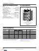
1.0V Output Transient Response 1.5V Output Transient Response 2.5V Output Transient Response
Efficiency vs Load Current from
5V
IN
(One Channel Operating)
Efficiency vs Load Current from
12V
IN
(One Channel Operating)
DCM Mode Efficiency from
1.5V
OUT
ELECTRICAL CHARACTERISTICS
Note 1: Stresses beyond those listed under Absolute Maximum Ratings
may cause permanent damage to the device. Exposure to any Absolute
Maximum Rating condition for extended periods may affect device
reliability and lifetime.
Note 2: The LTM4644E/LTM4644E-1 is tested under pulsed load
conditions such that T
J
≈ T
A
. The LTM4644E/LTM4644-1 is guaranteed to
meet performance specifications over the 0°C to 125°C internal operating
temperature range. Specifications over the full –40°C to 125°C internal
operating temperature range are assured by design, characterization and
correlation with statistical process controls. The LTM4644I/LTM4644I-1
is guaranteed to meet specifications over the full –40°C to 125°C internal
operating temperature range. The LTM4644MP/LTM4644MP-1 is tested
and guaranteed over full –55°C to 125°C internal operating temperature
range. Note that the maximum ambient temperature consistent with
these specifications is determined by specific operating conditions in
conjunction with board layout, the rated package thermal resistance and
other environmental factors.
Note 3: 100% tested at wafer level.
Note 4: See output current derating curves for different V
IN
, V
OUT
and T
A
.
Note 5: This IC includes overtemperature protection that is intended
to protect the device during momentary overload conditions. Junction
temperature will exceed 125°C when overtemperature protection is active.
Continuous operation above the specified maximum operating junction
temperature may impair device reliability.
TYPICAL PERFORMANCE CHARACTERISTICS
LOAD CURRENT (A)
0
70
EFFICIENCY (%)
75
85
90
95
100
1
4644 G01
80
4
2
3
3.3V
OUT
2.5V
OUT
1.8V
OUT
1.5V
OUT
1.2V
OUT
LOAD CURRENT (A)
0
65
EFFICIENCY (%)
70
80
85
90
95
1
4644 G02
75
4
2
3
5V
OUT
3.3V
OUT
2.5V
OUT
1.8V
OUT
1.5V
OUT
1.2V
OUT
LOAD CURRENT (A)
0.001
0
EFFICIENCY (%)
20
30
40
100
0.01
4644 G03
10
50
60
70
80
90
100.1 1
5V
IN
12V
IN
20µs/DIV
LOAD STEP
1A/DIV
4644 G04
V
OUT
50mV/DIV
AC-COUPLED
V
IN
= 12V, V
OUT
= 1V, I
OUT
= 3A TO 4A, 1A/µs
C
FF
= 10pF
OUTPUT CAPACITOR = 1 • 47µF CERAMIC
(Per Channel)
20µs/DIV
LOAD STEP
1A/DIV
4644 G05
V
OUT
50mV/DIV
AC-COUPLED
V
IN
= 12V, V
OUT
= 1.5V, I
OUT
= 3A TO 4A, 1A/µs
C
FF
= 10pF
OUTPUT CAPACITOR = 1 • 47µF CERAMIC
20µs/DIV
LOAD STEP
1A/DIV
4644 G06
V
OUT
50mV/DIV
AC-COUPLED
V
IN
= 12V, V
OUT
= 2.5V, I
OUT
= 3A TO 4A, 1A/µs
C
FF
= 10pF
OUTPUT CAPACITOR = 1 • 47µF CERAMIC
Downloaded from Arrow.com.Downloaded from Arrow.com.Downloaded from Arrow.com.Downloaded from Arrow.com.