
Datasheet


LTM4644/LTM4644-1
6
Rev. F
For more information www.analog.com
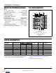
PIN FUNCTIONS
V
OUT1
(A1, A2, A3), V
OUT2
(C1, D1, D2), V
OUT3
(F1,
G1, G2), V
OUT4
(J1, K1, K2): Power Output Pins of Each
Switching Mode Regulator Channel. Apply output load
between these pins and GND pins. Recommend placing
output decoupling capacitance directly between these pins
and GND pins. See the Applications Information section
for paralleling outputs.
GND (A4-A5, B1-B2, C5, D3-D5, E1-E2, F5, G3-G5,
H1-H2, J5, K3-K4, L1-L2): Power Ground Pins for Both
Input and Output Returns. Use large PCB copper areas to
connect all GND together.
V
IN1
(B3, B4), V
IN2
(E3, E4), V
IN3
(H3, H4), V
IN4
(L3, L4):
Power input
pins connect to the drain of the internal top
MOSFET for each switching mode regulator channel.
Apply input voltages between these pins and GND pins.
Recommend placing input decoupling capacitance directly
between each of V
IN
pins and GND pins.
PGOOD1, PGOOD2, PGOOD3, PGOOD4 (C3, C2, F2,
J2): Output Power Good with Open-Drain Logic of Each
Switching Mode Regulator Channel. PGOOD is pulled to
ground when the voltage on the FB pin is not within ±10%
of the internal 0.6V reference.
CLKOUT
(J3): Output Clock Signal for PolyPhase
®
Opera-
tion of
the Module. The phase of CLKOUT with respect to
CLKIN is set to 180°. CLKOUT’s peak-to-peak amplitude
is INTV
CC
to GND. See the Application Information section
for details. Strictly output; do not drive this pin.
INTV
CC1
, INTV
CC2
, INTV
CC3
, INTV
CC4
(C4, F4, J4, K5):
Internal 3.3V Regulator Output of Each Switching Mode
Regulator Channel. The internal power drivers and con
-
trol circuits are powered from this voltage. Each pin is
internally decoupled to GND with 1µF low ESR ceramic
capacitor already.
SV
IN1
, SV
IN2
, SV
IN
, SV
IN4
(B5, E5, H5, L5): Signal V
IN
.
Filtered input voltage to the internal 3.3V regulator for
the control circuitry of each Switching mode Regulator
Channel. Tie this pin to the V
IN
pin respectively in most
applications. Connect SV
IN
to an external voltage supply
of at least 4V which must also be greater than V
OUT
.
TRACK/SS1, TRACK/SS2, TRACK/SS3, TRACK/SS4 (A6,
D6, G6, K6): Output Tracking and Soft-Start Pin of Each
Switching Mode Regulator Channel. Allows the user to
control the rise time of the output voltage. Putting a volt-
age below
0.6V on this pin bypasses the internal reference
input to the error amplifier, instead it servos the FB pin
to match the TRACK voltage. Above 0.6V, the tracking
function stops and the internal reference resumes control
of the error amplifier. There’s an internal 2.5µA pull-up
current from INTV
CC
on this pin, so putting a capacitor
here provides soft-start function.
MODE1, MODE2, MODE3, MODE4 (B6, E6, H6, L6):
Operation Mode Select for Each Switching Mode Regula
-
tor Channel
. Tie this pin to INTV
CC
to force continuous
synchronous operation at all output loads. Tying it to
SGND enables discontinuous current mode operation at
light loads. Do not leave floating.
RUN1, RUN2, RUN3, RUN4 (C6, F6, J6, K7): Run Control
Input of Each Switching Mode Regulator Channel. Enable
regulator operation by tying the specific RUN pin above
1.2V. Pulling it below 1.1V shuts down the respective
regulator channel. Do not leave floating.
FB1, FB2, FB3, FB4 (A7, D7, G7, J7): The Negative Input
of the Error Amplifier for Each Switching Mode Regulator
Channel. Internally, in LTM4644, this pin is connected to
V
OUT
of each channel with a 60.4kΩ precision resistor.
Different output voltages can be programmed
with an
additional resistor between the FB and GND pins for the
LTM4644, and two resistors between the V
OUT
, FB and
GND pins for the LTM4644-1. In PolyPhase operation, tying
the FB pins together allows for parallel operation. See the
Applications Information section for details.
PACKAGE ROW AND COLUMN LABELING M AY VARY
AMONG µModule PRODUCTS. REVIEW EACH PACKAGE
LAYOUT CAREFULLY.
Downloaded from Arrow.com.Downloaded from Arrow.com.Downloaded from Arrow.com.Downloaded from Arrow.com.Downloaded from Arrow.com.Downloaded from Arrow.com.