
Datasheet


LTM4644/LTM4644-1
7
Rev. F
For more information www.analog.com
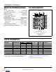
PIN FUNCTIONS
COMP1, COMP2, COMP3, COMP4 (B7, E7, H7, L7): Cur-
rent Control
Threshold and Error Amplifier Compensation
Point of Each Switching Mode Regulator Channel. The
internal current comparator threshold is proportional to
this voltage. Tie the COMP pins together for parallel opera
-
tion. The device is internally compensated.
CLKIN
(C7): External Synchronization Input to Phase
Detector of the Module. This pin is internally terminated
to SGND with 20kΩ. The phase-locked loop will force
the channel 1 turn-on signal to be synchronized with the
rising edge of the CLKIN signal. Channel 2, channel 3 and
channel 4 will also be synchronized with the rising edge of
the CLKIN signal with a pre-determined phase shift. See
the Applications Information section for details.
SGND (F7): Signal Ground Connection. SGND is connected
to GND internally through single point. Use a separated
SGND ground copper area for the ground of the feedback
resistor and other components connected to signal pins.
A second connection between the PGND plane and SGND
plane is recommended on the backside of the PCB under
-
neath the module.
TEMP
(F3): Onboard Temperature Diode for Monitoring
the VBE Junction Voltage Change with Temperature. See
the Applications Information section.
Downloaded from Arrow.com.Downloaded from Arrow.com.Downloaded from Arrow.com.Downloaded from Arrow.com.Downloaded from Arrow.com.Downloaded from Arrow.com.Downloaded from Arrow.com.