
Datasheet

LTM8001
18
8001fb
For more information www.linear.com/LTM8001
inductor value is 2.2uH. If the LTM8001 negative current
limit is set to 5A, for example, the energy that the input
capacitance must absorb is 1/2 LI
2
= 27.5μJ. Suppose
the comparator circuit in Figure 5d is set to pull the RUN
pin down when V
TRIP
= 15V. The input voltage will rise
according to the capacitor energy equation:
1
2
C V
IN
2
– V
TRIP
2
( )
= 27.5µJ
If the total input capacitance is 10μF, the input voltage
will rise to:
27.5µJ=
1
2
10µF V
IN
2
–15V
2
( )
V
IN
= 15.2V
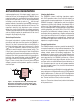
PCB Layout
Most of the headaches associated with PCB layout have
been alleviated or even eliminated by the high level of
integration of the LTM8001. The LTM8001 is neverthe
-
less a switching power supply, and care must be taken to
minimize EMI and ensure proper operation. Even with the
high level of integration, you may fail to achieve specified
operation with a haphazard or poor layout. See Figure 6
for a suggested layout. Ensure that the grounding and heat
sinking are acceptable. A few rules to keep in mind are:
1.
Place the R
SETx
, R
FB0
and R
T
resistors as close as pos-
sible to their respective pins.
2.
Place the C
IN0
capacitor as close as possible to the V
IN0
and GND connection of the LTM8001.
3. Place the ceramic C
OUT0
capacitor as close as possible
to the V
OUT0
and GND connection of the LTM8001. The
electrolytic C
OUT0
capacitor may be farther from the
LTM8001. Place the remaining C
OUTx
output capacitors
as close as possible to the V
OUTx
pins.
4. Place the C
IN0
and C
OUT0
capacitors such that their
ground currents flow directly adjacent or underneath
the LTM8001.
5. Connect all of the GND connections to as large a copper
pour or plane area as possible on the top layer. Avoid
breaking the ground connection between the external
components and the LTM8001.
6. Use vias to connect the GND copper area to the board’s
internal ground planes. Liberally distribute these GND
vias to provide both a good ground connection and
thermal path to the internal planes of the printed circuit
board. Pay attention to the location and density of the
thermal vias in Figure 6. The LTM8001 can benefit from
the heat sinking afforded by vias that connect to internal
GND planes at these locations, due to their proximity
to internal power handling components. The optimum
number of thermal vias depends upon the printed
circuit board design. For example, a board might use
very small via holes. It should employ more thermal
vias than a board that uses larger holes.
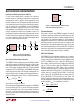
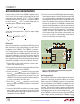
APPLICATIONS INFORMATION
Figure 6. Layout Showing Suggested External Components,
GND Plane and Thermal Vias
Hot Plugging Safely
The small size, robustness and low impedance of ceramic
capacitors make them an attractive option for the input
bypass capacitor of LTM8001. However, these capacitors
can cause problems if the LTM8001 is plugged into a live
input supply (see Application Note 88 for a complete dis
-
cussion). The low loss ceramic capacitor combined with
stray inductance in series with the power source forms an
underdamped tank circuit, and the voltage at the V
IN0
pin
of the LTM8001 can ring to more than twice the nominal
input voltage, possibly exceeding the LTM8001’s rating
V
OUT1
V
IN0
V
REF
SYNC RT
COMP
FBO
SS RUN
I
LIM
V
OUT2
V
OUT3
V
OUT4
V
OUT5
V
IN45
V
OUT0
C
OUT0
C
OUT5
GND
8001 F06
GND
C
IN0
THERMAL VIAS
SET5
SET4 SET3 SET2
SET1
BIAS45
BIAS123
C
OUT1
C
OUT2
C
OUT3
C
OUT4
GNDGND