LTM9008-14/ LTM9007-14/LTM9006-14 14-Bit, 65Msps/40Msps/ 25Msps Low Power Octal ADCs FEATURES n n n n n n n n n n n n DESCRIPTION 8-Channel Simultaneous Sampling ADC 73dB SNR 90dB SFDR Low Power: 88mW/59mW/46mW per Channel Single 1.8V Supply Serial LVDS Outputs: 1 or 2 Bits per Channel Selectable Input Ranges: 1VP-P to 2VP-P 800MHz Full Power Bandwidth S/H Shutdown and Nap Modes Serial SPI Port for Configuration Internal Bypass Capacitance, No External Components 140-Pin (11.
LTM9008-14/ LTM9007-14/LTM9006-14 ABSOLUTE MAXIMUM RATINGS PIN CONFIGURATION (Notes 1, 2) Supply Voltages VDD, OVDD................................................. –0.3V to 2V Analog Input Voltage (AIN+, AIN –, PAR/SER, SENSE) (Note 3)........... –0.3V to (VDD + 0.2V) Digital Input Voltage (ENC+, ENC–, CS, SDI, SCK) (Note 4)..................................... –0.3V to 3.9V SDO (Note 4).............................................. –0.3V to 3.9V Digital Output Voltage................. –0.
LTM9008-14/ LTM9007-14/LTM9006-14 CONVERTER CHARACTERISTICS The l denotes the specifications which apply over the full operating temperature range, otherwise specifications are at TA = 25°C. (Note 5) PARAMETER LTM9008-14 MIN TYP MAX CONDITIONS Resolution (No Missing Codes) l LTM9007-14 MIN TYP MAX 14 LTM9006-14 MIN TYP MAX 14 UNITS 14 Bits Integral Linearity Error Differential Analog Input (Note 6) l –4.1 ±1.2 4.1 –2.75 ±1 2.75 –2.75 ±1 2.
LTM9008-14/ LTM9007-14/LTM9006-14 DYNAMIC ACCURACY The l denotes the specifications which apply over the full operating temperature range, otherwise specifications are at TA = 25°C. AIN = –1dBFS. (Note 5) SYMBOL PARAMETER CONDITIONS LTM9008-14 MIN TYP MAX LTM9007-14 MIN TYP MAX LTM9006-14 MIN TYP MAX UNITS SNR Signal-to-Noise Ratio 5MHz Input 30MHz Input 70MHz Input 140MHz Input 73.7 73.7 73.5 73 73.5 73.4 73.4 72.8 72.9 72.9 72.8 72.
LTM9008-14/ LTM9007-14/LTM9006-14 DIGITAL INPUTS AND OUTPUTS The l denotes the specifications which apply over the full operating temperature range, otherwise specifications are at TA = 25°C. (Note 5) SYMBOL PARAMETER CONDITIONS MIN TYP MAX UNITS ENCODE INPUTS (ENC+, ENC– ) Differential Encode Mode (ENC– Not Tied to GND) VID Differential Input Voltage (Note 8) l 0.2 VICM Common Mode Input Voltage Internally Set Externally Set (Note 8) l 1.1 l 0.
LTM9008-14/ LTM9007-14/LTM9006-14 POWER REQUIREMENTS The l denotes the specifications which apply over the full operating temperature range, otherwise specifications are at TA = 25°C. (Note 9) SYMBOL PARAMETER CONDITIONS LTM9008-14 MIN TYP MAX LTM9007-14 MIN TYP MAX LTM9006-14 MIN TYP MAX UNITS 1.9 1.7 1.9 1.7 1.7 1.7 VDD Analog Supply Voltage (Note 10) l 1.7 OVDD Output Supply Voltage (Note 10) l 1.7 1.8 1.9 1.8 1.9 1.8 1.
LTM9008-14/ LTM9007-14/LTM9006-14 TIMING CHARACTERISTICS The l denotes the specifications which apply over the full operating temperature range, otherwise specifications are at TA = 25°C.
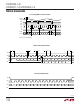
LTM9008-14/ LTM9007-14/LTM9006-14 TIMING DIAGRAMS 2-Lane Output Mode, 16-Bit Serialization* tAP ANALOG INPUT N+1 N tENCH ENC– tENCL ENC+ tSER DCO– DCO+ tFRAME FR– FR+ tDATA tSER tPD OUT#A– OUT#A+ OUT#B– OUT#B+ tSER D5 D3 D1 0 D13 D11 D9 D7 D5 D3 D1 0 D13 D11 D9 D4 D2 D0 0 D12 D10 D8 D6 D4 D2 D0 0 D12 D10 D8 SAMPLE N-6 SAMPLE N-5 SAMPLE N-4 90067814 TD01 *SEE THE DIGITAL OUTPUTS SECTION 2-Lane Output Mode, 14-Bit Serialization tAP ANALOG INPUT N+2 N tENCH ENC– N+
LTM9008-14/ LTM9007-14/LTM9006-14 TIMING DIAGRAMS 2-Lane Output Mode, 12-Bit Serialization tAP ANALOG INPUT N N+1 tENCH ENC– tENCL ENC+ tSER DCO– DCO+ FR+ tFRAME tDATA tPD tSER FR– OUT#A– OUT#A+ OUT#B– OUT#B+ tSER D9 D7 D5 D3 D13 D11 D9 D7 D5 D3 D13 D11 D9 D8 D6 D4 D2 D12 D10 D8 D6 D4 D2 D12 D10 D8 SAMPLE N-6 SAMPLE N-5 SAMPLE N-4 90067814 TD03 1-Lane Output Mode, 16-Bit Serialization tAP ANALOG INPUT N+1 N tENCH ENC– tENCL ENC+ tSER DCO– DCO+ tFRAME FR– FR+ OUT#A–
LTM9008-14/ LTM9007-14/LTM9006-14 TIMING DIAGRAMS 1-Lane Output Mode, 12-Bit Serialization tAP ANALOG INPUT N+1 N tENCH ENC– tENCL ENC+ tSER DCO– DCO+ tFRAME FR– FR+ OUT#A– OUT#A+ tDATA tSER tPD D5 D4 D3 tSER D2 D13 D12 D11 D10 D9 SAMPLE N-6 D8 D7 D6 D5 D4 D3 D2 D13 D12 D11 SAMPLE N-5 SAMPLE N-4 90067814 TD07 OUT#B+, OUT#B– ARE DISABLED SPI Port Timing (Readback Mode) tDS tS tDH tSCK tH CS SCK tDO SDI SDO R/W A6 A5 A4 A3 A2 A1 A0 XX D7 HIGH IMPEDANCE XX D6 XX D5
LTM9008-14/ LTM9007-14/LTM9006-14 TYPICAL PERFORMANCE CHARACTERISTICS LTM9008-14: Integral Nonlinearity (INL) vs Output Code LTM9008-14: Differential Nonlinearity (DNL) vs Output Code 2.0 1.5 0 0.4 –10 –20 0.3 0.5 0 –0.5 –1.0 –30 0.2 AMPLITUDE (dBFS) DNL ERROR (LSB) 1.0 0.1 0 –0.1 –0.2 –1.5 –0.4 –2.0 –0.
LTM9008-14/ LTM9007-14/LTM9006-14 TYPICAL PERFORMANCE CHARACTERISTICS LTM9008-14: SNR vs Input Frequency, –1dBFS, 2V Range, 65Msps LTM9008-14: SFDR vs Input Frequency, –1dBFS, 2V Range, 65Msps 74 110 95 100 73 90 70 69 SFDR (dBc AND dBFS) SFDR (dBFS) SNR (dBFS) 71 85 80 75 68 80 70 60 dBc 50 40 30 20 70 67 dBFS 90 72 66 LTM9008-14: SFDR vs Input Level, fIN = 70MHz, 2V Range, 65Msps 10 0 50 100 150 200 250 300 INPUT FREQUENCY (MHz) 65 350 0 50 100 150 200 250 300 INPUT FREQUEN
LTM9008-14/ LTM9007-14/LTM9006-14 TYPICAL PERFORMANCE CHARACTERISTICS LTM9007-14: Integral Nonlinearity (INL) vs Output Code LTM9007-14: Differential Nonlinearity (DNL) vs Output Code 0.5 2.0 1.5 –20 0.3 0.5 0 –0.5 –1.0 0.2 AMPLITUDE (dBFS) DNL ERROR (LSB) 1.0 0.1 0 –0.1 –0.2 –30 –40 –50 –60 –70 –80 –90 –0.3 –100 –1.5 –0.4 –110 –2.0 –0.
LTM9008-14/ LTM9007-14/LTM9006-14 TYPICAL PERFORMANCE CHARACTERISTICS LTM9007-14: SNR vs Input Frequency, –1dBFS, 2V Range, 40Msps LTM9007-14: SFDR vs Input Frequency, –1dBFS, 2V Range, 40Msps LTM9007-14: SFDR vs Input Level, fIN = 70MHz, 2V Range, 40Msps 95 74 110 100 73 90 70 69 SFDR (dBc AND dBFS) SFDR (dBFS) SNR (dBFS) 72 71 85 80 75 68 66 80 70 60 dBc 50 40 30 20 70 67 dBFS 90 10 0 50 100 150 200 250 300 INPUT FREQUENCY (MHz) 350 65 0 100 150 200 250 300 INPUT FREQUENCY (MH
LTM9008-14/ LTM9007-14/LTM9006-14 TYPICAL PERFORMANCE CHARACTERISTICS LTM9006-14: Integral Nonlinearity (INL) vs Output Code LTM9006-14: Differential Nonlinearity (DNL) vs Output Code 0.5 2.0 0 –10 0.4 1.5 –20 0.3 0.5 0 –0.5 –1.0 0.2 AMPLITUDE (dBFS) DNL ERROR (LSB) 1.0 0.1 0 –0.1 –0.2 –0.4 –2.0 –0.
LTM9008-14/ LTM9007-14/LTM9006-14 TYPICAL PERFORMANCE CHARACTERISTICS LTM9006-14: SNR vs Input Frequency, –1dBFS, 2V Range, 25Msps LTM9006-14: SFDR vs Input Frequency, –1dBFS, 2V Range, 25Msps 74 LTM9006-14: SFDR vs Input Level, fIN = 70MHz, 2V Range, 25Msps 95 110 100 73 90 70 69 SFDR (dBc AND dBFS) SFDR (dBFS) SNR (dBFS) 72 71 85 80 75 68 66 0 100 150 200 250 300 INPUT FREQUENCY (MHz) 50 350 dBc 60 50 40 30 0 50 100 150 200 250 300 INPUT FREQUENCY (MHz) DCO Cycle-Cycle Jitter vs S
LTM9008-14/ LTM9007-14/LTM9006-14 PIN FUNCTIONS AIN1+ (B2): Channel 1 Positive Differential Analog Input. AIN8+ (N1): Channel 8 Positive Differential Analog Input. AIN1– (B1): Channel 1 Negative Differential Analog Input. AIN8– (N2): Channel 8 Negative Differential Analog Input VCM12 (B3): Common Mode Bias Output, Nominally Equal to VDD/2. VCM should be used to bias the common mode of the analog inputs of channels 1 and 2. VCM is internally bypassed to ground with a 0.1µF ceramic capacitor.
LTM9008-14/ LTM9007-14/LTM9006-14 PIN FUNCTIONS OVDD (G9, G10): Output Driver Supply. OVDD is internally bypassed to ground with a 0.1µF ceramic capacitor. SDOA (E6): In serial programming mode, (PAR/SER = 0V), SDOA is the optional serial interface data output for registers controlling channels 1, 4, 5 and 8. Data on SDO is read back from the mode control registers and can be latched on the falling edge of SCK.
LTM9008-14/ LTM9007-14/LTM9006-14 PIN CONFIGURATION TABLE 1 2 3 4 5 6 7 8 9 10 A GND GND GND GND GND GND PAR/SER O2A+ GND GND B AIN1– AIN1+ VCM12 GND GND VREF GND O2A– GND GND C – AIN2 + AIN2 GND GND SENSE GND O2B+ O1B– O4A– O4A+ D GND GND VDD VDD GND SDOB O2B– O1B+ O3A+ O3A– E AIN3– AIN3+ VDD VDD GND SDOA O1A– O1A+ O3B+ O3B– F GND GND VCM34 GND GND GND O4B– O4B+ DCOB+ DCOB– G AIN4– AIN4+ GND GND GND GND DCOA+ DCOA– OVDD
LTM9008-14/ LTM9007-14/LTM9006-14 FUNCTIONAL BLOCK DIAGRAM VDD = 1.8V OVDD = 1.
LTM9008-14/ LTM9007-14/LTM9006-14 APPLICATIONS INFORMATION CONVERTER OPERATION INPUT DRIVE CIRCUITS The LTM9008-14/LTM9007-14/LTM9006-14 are low power, 8-channel, 14-bit, 65Msps/40Msps/25Msps A/D converters that are powered by a single 1.8V supply. The analog inputs should be driven differentially. The encode input can be driven differentially for optimal jitter performance, or single-ended for lower power consumption. The digital outputs are serial LVDS to minimize the number of data lines.
LTM9008-14/ LTM9007-14/LTM9006-14 APPLICATIONS INFORMATION Amplifier Circuits Figure 7 shows the analog input being driven by a high speed differential amplifier. The output of the amplifier is AC-coupled to the A/D so the amplifier’s output common mode voltage can be optimally set to minimize distortion. See back page for a DC-coupled example. 50Ω At very high frequencies an RF gain block will often have lower distortion than a differential amplifier.
LTM9008-14/ LTM9007-14/LTM9006-14 APPLICATIONS INFORMATION Reference The input range can be adjusted by applying a voltage to SENSE that is between 0.625V and 1.30V. The input range will then be 1.6 • VSENSE. The reference is shared by all eight ADC channels, so it is not possible to independently adjust the input range of individual channels. The LTM9008-14/LTM9007-14/LTM9006-14 has an internal 1.25V voltage reference. For a 2V input range using the internal reference, connect SENSE to VDD.
LTM9008-14/ LTM9007-14/LTM9006-14 APPLICATIONS INFORMATION Encode Input The signal quality of the encode inputs strongly affects the A/D noise performance. The encode inputs should be treated as analog signals—do not route them next to digital traces on the circuit board. There are two modes of operation for the encode inputs: the differential encode mode (Figure 10), and the single-ended encode mode (Figure 11).
LTM9008-14/ LTM9007-14/LTM9006-14 APPLICATIONS INFORMATION input. ENC+ can be taken above VDD (up to 3.6V) so 1.8V to 3.3V CMOS logic levels can be used. The ENC+ threshold is 0.9V. For good jitter performance ENC+ should have fast rise and fall times. Clock PLL and Duty Cycle Stabilizer The encode clock is multiplied by an internal phase-locked loop (PLL) to generate the serial digital output data. If the encode signal changes frequency or is turned off, the PLL requires 25µs to lock onto the input clock.
LTM9008-14/ LTM9007-14/LTM9006-14 APPLICATIONS INFORMATION Programmable LVDS Output Current The default output driver current is 3.5mA. This current can be adjusted by control register A2 in the serial programming mode. Available current levels are 1.75mA, 2.1mA, 2.5mA, 3mA, 3.5mA, 4mA and 4.5mA. In the parallel programming mode, the SCK pin can select either 3.5mA or 1.75mA.
LTM9008-14/ LTM9007-14/LTM9006-14 APPLICATIONS INFORMATION Digital Output Test Pattern DEVICE PROGRAMMING MODES To allow in-circuit testing of the digital interface to the A/D, there is a test mode that forces the A/D data outputs (D13-D0) of all channels to known values. The digital output test patterns are enabled by serially programming mode control registers A3 and A4. When enabled, the test patterns override all other formatting modes: 2’s complement and randomizer.
LTM9008-14/ LTM9007-14/LTM9006-14 APPLICATIONS INFORMATION Serial Programming Mode To use the serial programming mode, PAR/SER should be tied to ground. The CS, SCK, SDI and SDO pins become a serial interface that program the A/D mode control registers. Data is written to a register with a 16-bit serial word. Data can also be read back from a register to verify its contents. Serial data transfer starts when CS is taken low. The data on the SDI pin is latched at the first 16 rising edges of SCK.
LTM9008-14/ LTM9007-14/LTM9006-14 APPLICATIONS INFORMATION REGISTER A1 (CSB): FORMAT AND POWER-DOWN REGISTER (ADDRESS 01h with CSB = GND) D7 D6 D5 D4 D3 D2 D1 D0 DCSOFF RAND TWOSCOMP SLEEP NAP_7 NAP_6 NAP_3 NAP_2 Note That CSA Controls Channels 1, 4, 5 and 8, CSB Controls Channels 2, 3, 6 and 7. Bit 7 DCSOFF Clock Duty Cycle Stabilizer Bit 0 = Clock Duty Cycle Stabilizer On 1 = Clock Duty Cycle Stabilizer Off. This Is Not Recommended.
LTM9008-14/ LTM9007-14/LTM9006-14 APPLICATIONS INFORMATION REGISTER A3: TEST PATTERN MSB REGISTER (ADDRESS 03h) D7 D6 D5 D4 D3 D2 D1 D0 OUTTEST X TP13 TP12 TP11 TP10 TP9 TP8 Note That CSA Controls Channels 1, 4, 5 and 8, CSB Controls Channels 2, 3, 6 and 7. Bit 7 OUTTEST Digital Output Test Pattern Control Bit 0 = Digital Output Test Pattern Off 1 = Digital Output Test Pattern On Bit 6 Unused, Don’t Care Bit.
LTM9008-14/ LTM9007-14/LTM9006-14 APPLICATIONS INFORMATION Table 5 lists the trace lengths for the analog inputs and digital outputs inside the package from the die pad to the package pad. These should be added to the PCB trace lengths for best matching. The material used for the substrate is BT (bismaleimidetriazine), supplied by Mitsubishi Gas and Chemical. In the DC to 125MHz range, the speed for the analog input signals is 198ps/in or 7.795ps/mm. The speed for the digital outputs is 188.5ps/in or 7.
LTM9008-14/ LTM9007-14/LTM9006-14 TYPICAL APPLICATIONS Silkscreen Top Inner Layer 2 Top Side Inner Layer 3 90067814f 32
LTM9008-14/ LTM9007-14/LTM9006-14 TYPICAL APPLICATIONS Inner Layer 4 Inner Layer 5 Bottom Side Silkscreen Bottom 90067814f 33
CLK+ CLK+ GND E4 E3 C3 0.01µF V+ 3V TO 6V J1 J2 R26 (OPT) R48 100Ω R27 (OPT) +1.8V C17 R37 (OPT) 0Ω 0805 R36 0Ω 0603 R15 (OPT) C10 4.7µF 6.3V 0603 R16 (OPT) C12 1µF 0603 C4 T1 R19 0.01µF MABA100Ω 007159-000000 5 1 2 C6 C9 0.01µF C8 4 3 0.01µF (OPT) 0.
2.000 2.000 SUGGESTED PCB LAYOUT TOP VIEW 1.200 aaa Z 0.4 Ø 140x 0.000 PACKAGE TOP VIEW 0.400 4 0.400 PIN “A1” CORNER 2.800 E 1.200 X D Information furnished by Linear Technology Corporation is believed to be accurate and reliable. However, no responsibility is assumed for its use. Linear Technology Corporation makes no representation that the interconnection of its circuits as described herein will not infringe on existing patent rights. 5.200 4.400 3.600 2.800 2.000 1.200 0.400 0.
LTM9008-14/ LTM9007-14/LTM9006-14 TYPICAL APPLICATION Single-Ended to Differential Conversion Using LTC6409 and 50MHz Lowpass Filter (Only One Channel Shown). Filter for Use at 61.44Msps 0.8pF 1.8V 1.8V 0.1µF IN– 150Ω 49.9Ω + 68pF 150pF LTC6409 – SHDN 37.4Ω VOCM 474Ω 180nH 150pF 180nH 100pF O1A+ E8 B1 AIN1 – O1A– E7 B3 DCO+ G7 75Ω C1 F2 GND F1 50Ω VDD + B2 AIN1 C2 0.8pF 66.9Ω 75Ω 33pF 68pF OUT+ B6 VREF OUT – 180nH SENSE IN+ 180nH ••• 0.1µF C5 37.