
Datasheet


17
90067814f
LTM9008-14/
LTM9007-14/LTM9006-14
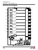
PIN FUNCTIONS
A
IN1
+
(B2): Channel 1 Positive Differential Analog Input.
A
IN1
–
(B1): Channel 1 Negative Differential Analog Input.
V
CM12
(B3): Common Mode Bias Output, Nominally Equal
to V
DD
/2. V
CM
should be used to bias the common mode
of the analog inputs of channels 1 and 2. V
CM
is internally
bypassed to ground with a 0.1µF ceramic capacitor. No
external capacitance
is required.
A
IN2
+
(C2): Channel 2 Positive Differential Analog Input.
A
IN2
–
(C1): Channel 2 Negative Differential Analog Input.
A
IN3
+
(E2): Channel 3 Positive Differential Analog Input.
A
IN3
–
(E1): Channel 3 Negative Differential Analog Input.
V
CM34
(F3): Common Mode Bias Output, Nominally Equal
to V
DD
/2. V
CM
should be used to bias the common mode
of the analog inputs of channels 3 and 4. V
CM
is internally
bypassed to ground with a 0.1µF ceramic capacitor. No
external capacitance is required.
A
IN4
+
(G2): Channel 4 Positive Differential Analog Input.
A
IN4
–
(G1): Channel 4 Negative Differential Analog Input.
A
IN5
+
(H1): Channel 5 Positive Differential Analog Input.
A
IN5
–
(H2): Channel 5 Negative Differential Analog Input.
V
CM56
(J3): Common Mode Bias Output, Nominally Equal
to V
DD
/2. V
CM
should be used to bias the common mode
of the analog inputs of channels 5 and 6. V
CM
is internally
bypassed to ground with a 0.1µF ceramic capacitor. No
external capacitance is required.
A
IN6
+
(K1): Channel 6 Positive Differential Analog Input.
A
IN6
–
(K2): Channel 6 Negative Differential Analog Input.
A
IN7
+
(M1): Channel 7 Positive Differential Analog Input.
A
IN7
–
(M2): Channel 7 Negative Differential Analog Input.
V
CM78
(N3): Common Mode Bias Output, Nominally Equal
to V
DD
/2. V
CM
should be used to bias the common mode
of the analog inputs of channels 7 and 8. V
CM
is internally
bypassed to ground with a 0.1µF ceramic capacitor. No
external capacitance is required.
A
IN8
+
(N1): Channel 8 Positive Differential Analog Input.
A
IN8
–
(N2): Channel 8 Negative Differential Analog Input
V
DD
(D3, D4, E3, E4, K3, K4, L3, L4): 1.8V Analog Power
Supply. V
DD
is internally bypassed to ground with 0.1μF
ceramic capacitors.
ENC
+
(P5): Encode Input. Conversion starts on the rising
edge.
ENC
–
(P6): Encode Complement Input. Conversion starts
on the falling edge.
CSA (L5): In serial programming mode, (PAR/SER = 0V),
CSA is the serial interface chip select input for registers
controlling channels 1, 4, 5 and 8. When
CS is low, SCK
is enabled for shifting data on SDI into the mode control
registers. In parallel programming mode (PAR/SER = V
DD
),
CS selects 2-lane or 1-lane output mode. CS can be driven
with 1.8V to 3.3V logic.
CSB (M5): In serial programming mode, (PAR/SER = 0V),
CSB is the serial interface chip select input for registers
controlling channels 2, 3, 6 and 7. When CS is low,
SCK
is enabled for shifting data on SDI into the mode control
registers. In parallel programming mode (PAR/SER = V
DD
),
CS selects 2-lane or 1-lane output mode. CS can be driven
with 1.8V to 3.3V logic.
SCK (L6): In serial programming mode, (PAR/SER =
0V), SCK is the serial interface clock input. In parallel
programming mode (PAR/SER = V
DD
), SCK selects 3.5mA
or 1.75mA LVDS
output currents. SCK can be driven with
1.8V to 3.3V logic.
SDI (M6): In serial programming mode, (PAR/SER = 0V),
SDI is the serial interface data Input. Data on SDI is clocked
into the mode control registers on the rising edge of SCK.
In parallel programming mode (PAR/SER = V
DD
), SDI can
be used to power down the part. SDI can be driven with
1.8V
to 3.3V logic.
GND (See Pin Configuration Table): ADC Power Ground.
Use multiple vias close to pins.