Photocoupler Product Data Sheet 6N135 / 6N136 series Spec No.: DS70-2008-0032 Effective Date: 12/15/2009 Revision: - LITE-ON DCC RELEASE BNS-OD-FC001/A4 LITE-ON Technology Corp. / Optoelectronics No.90,Chien 1 Road, Chung Ho, New Taipei City 23585, Taiwan, R.O.C. Tel: 886-2-2222-6181 Fax: 886-2-2221-1948 / 886-2-2221-0660 http://www.liteon.
LITE - O N TECH NO LO G Y CO RP O RATIO N Property of Lite-on Only 6N135, 6N136 Single Channel, High Speed Optocouplers Jan.2009 Description The 6N135/6 consists of a high efficient AlGaAs Light Emitting Diode and a high speed optical detector. This design provides excellent AC and DC isolation between the input and output sides of the Optocoupler. Connection for the bias of the photodiode improves the speed that of a conventional phototransistor coupler by reducing the base-collector capacitances.
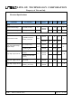
LITE - O N TECH NO LO G Y CO RP O RATIO N Property of Lite-on Only Ordering Information Minimum CMR Part Option dV/dt (V/μs) VCM (V) CTR Remarks Single Channel, DIP-8 6N135 M S 6N136 7 1000 M S Part No.
LITE - O N TECH NO LO G Y CO RP O RATIO N Property of Lite-on Only Package Dimensions 8-pin DIP Package (6N135 / 6N136) *1. Year date code. *2. 2-digit work week. *3. Factory identification mark (Z : Taiwan, Y : Thailand). Dimensions are in Millimeters and (Inches). Part No.
LITE - O N TECH NO LO G Y CO RP O RATIO N Property of Lite-on Only Package Dimensions 8-pin DIP Wide Lead Spacing Package (6N135M / 6N136M) *1. Year date code. *2. 2-digit work week. *3. Factory identification mark (Z : Taiwan, Y : Thailand). Dimensions are in Millimeters and (Inches). Part No.
LITE - O N TECH NO LO G Y CO RP O RATIO N Property of Lite-on Only Package Dimensions 8-pin DIP Surface Mount Package (6N135S / 6N136S) *1. Year date code. *2. 2-digit work week. *3. Factory identification mark (Z : Taiwan, Y : Thailand). Dimensions are in Millimeters and (Inches). Part No.
LITE - O N TECH NO LO G Y CO RP O RATIO N Property of Lite-on Only Taping Dimensions 6N135S/136S-TA 6N137S-TA1 6N135S/136S-TA1 Description Symbol Dimensions in millimeters ( inches ) Tape wide W 16 0.3 ( .63 ) Pitch of sprocket holes P0 4 0.1 ( .15 ) Distance of compartment F P2 7.5 0.1 ( .295 ) 2 0.1 ( .079 ) Distance of compartment to compartment P1 12 0.1 ( .472 ) Part No.
LITE - O N TECH NO LO G Y CO RP O RATIO N Property of Lite-on Only Recommended Lead Free Reflow Profile Part No.
LITE - O N TECH NO LO G Y CO RP O RATIO N Property of Lite-on Only Absolute Maximum Ratings*1 Parameter Symbol Min Max TST -55 125 o 85 o Storage Temperature Operating Temperature TA -40 Isolation Voltage VISO 5000 Supply Voltage VCC Lead Solder Temperature * 2 Units Note C C VRMS 15 V 260 C 2 Input Average Forward Input Current IF 25 mA Reverse Input Voltage VR 5 V Input Power Dissipation PI 45 mW Output Collector Current IO 8 mA Output Collector Voltage VO 20
LITE - O N TECH NO LO G Y CO RP O RATIO N Property of Lite-on Only Electrical Specifications Parameters Test Condition Symbol Device Min Typ Max Units 1.4 1.7 V Input Input Forward Voltage IF =16mA, TA=25℃ Input Reverse Voltage IR = 10μA VF BVR 6N135 6N136 5 V Detector Current transfer ratio IF=16mA;Vcc=4.5V; TA=25℃;Vo=0.4V 6N135 IF IF=16mA;Vcc=4.5V; Io=1.1mA; TA=25℃ IF=16mA;Vcc=4.5V; Io=3mA; TA=25℃ IF=0mA, Vo=Vcc=15V TA=25℃ 50 % 19 24 50 6N135 0.18 0.4 6N136 0.25 0.
LITE - O N TECH NO LO G Y CO RP O RATIO N Property of Lite-on Only Switching Specifications TA=0~70℃, Vcc=5V, unless otherwise specified. Parameter Propagation Delay Time to Low Output Level Propagation Delay Time to High Output Level Logic High Common Mode Transient Immunity Logic Low Common Mode Transient Immunity Test Condition Symbol TA=25℃ (RL=4.1KΩ, IF=16mA) TA=25℃ (RL=1.9KΩ, IF=16mA) TA=25℃ (RL=4.1KΩ, IF=16mA) TA=25℃ (RL=1.9KΩ, IF=16mA) Min Typ Max Units 6N135 0.09 1.5 μs 6N136 0.
LITE - O N TECH NO LO G Y CO RP O RATIO N Property of Lite-on Only Isolation Characteristics Parameter Test Condition Symbol Input-Output Insulation Leakage Current 45% RH, t = 5s, o VI-O = 3kV DC, TA = 25 C II-O Withstand Insulation Test Voltage RH ≤ 50%, t = 1min, o TA = 25 C VISO Input-Output Resistance VI-O = 500V DC RI-O Min Typ Max Units 1.0 μA 5000 VRMS 12 Ω 10 *All Typical at TA =25℃ Notes 1. A 0.1µF or bigger bypass capacitor for VCC is needed as shown in Fig.1 2.
LITE - O N TECH NO LO G Y CO RP O RATIO N Property of Lite-on Only Switching Time Test Circuit Figure 1: Single Channel Test Circuit for tPHL and tPLH Figure 2: Single Channel Test Circuit for Common Mode Transient Immunity Part No.
LITE - O N TECH NO LO G Y CO RP O RATIO N Property of Lite-on Only Characteristics Curves Figure 3: DC and pulsed transfer characteristics Figure 6: Current transfer ratio vs. input current Figure 4: Input current vs. forward voltage Figure 7: Current transfer ratio vs. temperature Figure 5: Logic high output current vs. temperature Figure 8: Small-signal current transfer ratio vs. quiescent current Part No.
LITE - O N TECH NO LO G Y CO RP O RATIO N Property of Lite-on Only Characteristics Curves Figure 9: Propagation delay time vs. temperature Figure 10: Propagation delay time vs. load resistance TPLH6N135 TPLH6N136 TPHL6N136 TPHL6N135 Part No.
LITE - O N TECH NO LO G Y CO RP O RATIO N Property of Lite-on Only Notice Specifications of the products displayed herein are subject to change without notice. The products shown in this publication are designed for the general use in electronic applications such as office automation equipment, communications devices, audio/visual equipment, electrical instrumentation and application.