IrDAW Data 1.2 Low Power Compliant 115.2 kb/s Infrared Transceiver Technical Data Features • Ultra Small Surface Mount Package • Minimal Height: 2.5 mm • Vcc from 2.7 to 3.6 Volts • Withstands > 250 mVp-p Power Supply Ripple • LED Supply Voltage can Range from 2.7 to 6.
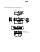
Applications Application Circuit VLED TXD RXD SHUT DOWN The HSDL-3201 meets the 20 cm link distance to other IrDA 1.2 low power devices, and a 30 cm link distance to IrDA 1.2 standard devices. VCC C1 1.0 µF 5 4 3 2 7 6 5 5 SD 3 2 VCC NC Pin 1 2 Symbol GND NC Description Ground No Connection 3 4 VCC AGND Supply Voltage Analog Ground 5 SD 6 RXD Receiver Data Output. Active Low. 7 TXD Transmitter Data Input. Active High.
Recommended Application Circuit Components Component C1 Recommended Value 1.0 µF Shutdown Mode Notes Note 1 Absolute Maximum Ratings For implementations where case to ambient thermal resistance is ≤ 50°C/W.
Recommended Operating Conditions Parameter Operating Temperature Supply Voltage LED Supply Voltage TXD, SD Input Logic High Voltage Logic Low Receiver Input Logic High Irradiance Logic Low Receiver Data Rate Symbol TA VCC VLED VIH VIL EIH EIL Min. -25 2.7 2.7 2/3 VCC 0 0.0081 2.4 RXD Output Waveform Conditions Notes For in-band signals. For in-band signals. 7 7 SD 90% RX LIGHT 50% VOL Units °C V V V V mW/cm2 µW/cm2 kb/s Receiver Wakeup Time Definition tpw VOH Max. 85 3.6 6.
Electrical & Optical Specifications Specifications hold over the recommended operating conditions unless otherwise noted. Unspecified test conditions may be anywhere in their operating range. All typical values are at 25°C and 3.0 V unless otherwise noted. Parameter Symbol Min. 2φ 1/2 30 Typ. Max. Units Conditions Note Receiver Viewing Angle Peak Sensitivity Wavelength RXD Output Voltage λp ° 880 nm Logic High VOH V CC -0.2 VCC V IOH =-200 µA, EI ≤ 0.3 µW/cm2 Logic Low VOL 0 0.
Notes: 1. C1, which is optional, must be placed within 0.7 cm of the HSDL-3201 to obtain optimum noise immunity. 2. If TXD is stuck in the high state, the LED will turn off after about 20 µs. 3. RXD will echo the TXD signal while TXD is transmitting data. 4. In-Band IrDA signals and data rates ≤ 115.2 Kb/s. 5. RXD Logic Low is a pulsed response. The pulse width is 2.4 µs, independent of data rate. 6. RXD Logic High during shutdown is a weak pullup resistor (300 kΩ). 7.
HSDL-3201#011/001/021 Package Dimensions MOUNTING CENTER 4.0 1.025 CL 2.05 RECEIVER EMITTER 2.2 2.5 1.175 0.35 0.65 0.80 1.05 1.25 2.85 2.55 4.0 8.0 3.0 2.9 1.85 CL UNIT: mm TOLERANCE: ± 0.2 mm COPLANARITY = 0.1 mm MAX. PIN 1 0.6 3.325 6.
HSDL-3201#011/001/021 Tape and Reel Dimensions UNIT: mm 4.0 ± 0.1 1.75 ± 0.1 + 0.1 ∅ 1.5 0 1.5 ± 0.1 POLARITY PIN 8: VLED 7.5 ± 0.1 16.0 ± 0.2 8.4 ± 0.1 PIN 1: GND 3.4 ± 0.1 0.4 ± 0.05 8.0 ± 0.1 2.8 ± 0.1 PROGRESSIVE DIRECTION EMPTY PARTS MOUNTED LEADER (400 mm MIN.) (40 mm MIN.) EMPTY (40 mm MIN.) OPTION # "B" "C" QUANTITY 001 178 60 500 021 330 80 2500 UNIT: mm DETAIL A 2.0 ± 0.5 B C ∅ 13.0 ± 0.5 R 1.0 LABEL 21 ± 0.8 DETAIL A 2 16.4 + 0 2.0 ± 0.
HSDL-3201#008/018 Package Dimensions +0.05 2.8 -0.2 3.6 2 1.55 1.55 +0.05 1.8 -0.2 2 CL 2.8 3.35 CL 0.4 ± 0.15 2.35 5.1 0.7 ± 0.1 7.5 Symbol GND NC VCC AGND SD RxD TxD VLED EMI Shield 3.325 0.95 x 7 = 6.65 ± 0.15 0.3 Pin 1 2 3 4 5 6 7 8 9 0.95 ± 0.1 0.6 ± 0.15 0 ± 0.05 (MAX.) Description Ground No Connection Supply Voltage Analog Ground Shutdown (Active High) Receive Data Transmit Data LED Voltage EMI Shield UNIT: mm TOLERANCE: ± 0.2 mm COPLANARITY = 0.1 mm MAX.
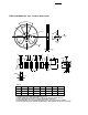
HSDL-3201#008/018 Tape and Reel Dimensions 60°TYP. ∅ 99.5 ± 1 120° 3 +0.5 ∅ 13.1 -0 ∅ 264 DETAIL A (5/1) PS ∅ 330 ± 1 1 2 Po D1 P2 Do +0.5 16.0 -0 B T E 2.6 F W A Bo 5° B-B SECTION 5°(MAX.) A P1 1.5 B Ao Ko 5°(MAX.) 5° 3.1 ± 0.1 A-A SECTION UNIT: mm SYMBOL SPEC SYMBOL SPEC Ao Bo Ko Po P1 P2 T 3.65 ± 0.10 7.90 ± 0.10 +0.05 2.75 - 0.10 4.00 ± 0.10 8.00 ± 0.10 2.00 ± 0.10 0.40 ± 0.10 E F Do D1 W 10Po 1.75 ± 0.10 7.50 ± 0.10 1.55 ± 0.05 1.50 (MIN.) 16.
Moisture Proof Packaging The HDSL-3201 is shipped in moisture proof packaging. Once opened, moisture absorption begins. Recommended Land Pattern for HSDL-3201#011/001/ 021 (Front Options) CL SHIELD SOLDER PAD 1.35 MOUNTING CENTER Recommended Storage Conditions Storage Temperature Relative Humidity 1.25 10°C to 30°C 2.05 0.10 below 60% RH 0.775 1.
Appendix A: HSDL-3201#011/001/021 SMT Assembly Application Note Solder Pad, Mask, and Metal Stencil METAL STENCIL FOR SOLDER PASTE PRINTING STENCIL APERTURE LAND PATTERN SOLDER MASK PCB Recommended Metal Solder Stencil Aperture It is recommended that only a 0.152 mm (0.006 inches) or a 0.127 mm (0.005 inches) thick stencil be used for solder paste printing. This is to ensure adequate printed solder paste volume and no shorting.
Adjacent Land Keep-out and Solder Mask Areas Adjacent land keep-out is the maximum space occupied by the unit relative to the land pattern. There should be no other SMD components within this area. 8.2 0.2 The minimum solder resist strip width required to avoid solder bridging adjacent pads is 0.2 mm. It is recommended that two fiducial crosses be place at mid-length of the pads for unit alignment. Note: Wet/Liquid Photo-Imageable solder resist/mask is recommended. 2.6 3.
PCB Layout Suggestion Component Side The following PCB layout shows a recommended layout that should result in good electrical and EMI performance. Things to note: 1. The ground plane should be continuous under the part, but should not extend under the shield trace. 2. The shield trace is a wide, low inductance trace back to the system ground. 5. VLED can be connected to either unfiltered or unregulated power.
Recommended Solder Paste/Cream Volume for Castellation Joints Based on calculation and experiment, the printed solder paste volume required per castellation pad is 0.22 cubic mm (based on either no-clean or aqueous solder cream types with typically 60% to 65% solid content by volume). Using the recommended stencil results in this volume of solder paste.
Reflow Profile MAX. 245°C T – TEMPERATURE – (°C) 230 R3 200 183 170 150 R2 90 sec. MAX. ABOVE 183°C 125 R1 100 R4 R5 50 25 0 50 100 150 200 250 300 t-TIME (SECONDS) P1 HEAT UP Process Zone Heat Up Solder Paste Dry Solder Reflow Cool Down Symbol P1, R1 P2, R2 P3, R3 P3, R4 P4, R5 The reflow profile is a straight line representation of a nominal temperature profile for a convective reflow solder process.
Window Design Minimum and Maximum Window Sizes To insure IrDA compliance, some constraints on the height and width of the window exist. The minimum dimensions ensure that the IrDA cone angles are met without vignetting. The maximum dimensions minimize the effects of stray light. The minimum size corresponds to a cone angle of 30 degrees, the maximum, to a cone angle of 60 degrees. Dimensions are in mm. Z Depth (Z) 0 1 2 3 4 5 6 7 8 9 10 Y min. 1.70 2.23 2.77 3.31 3.84 4.38 4.91 5.45 5.99 6.52 7.
Shape of the Window From an optics standpoint, the window should be flat. This ensures that the window will not alter either the radiation pattern of the LED, or the receive pattern of the photodiode. Flat Window (First choice) If the window must be curved for mechanical design reasons, place a curve on the back side of the window that has the same radius as the front side. While this will not completely eliminate the lens effect of the front curved surface, it will reduce the effects.
Test Methods Background Light and Electromagnetic Field There are four ambient interference conditions in which the receiver is to operate correctly. The conditions are to be applied separately: 1. Electromagnetic field: 3 V/m maximum (please refer to IEC 801-3, severity level 3 for details). 2. Sunlight: 10 kilolux maximum at the optical port.
www.agilent.com/semiconductors For product information and a complete list of distributors, please go to our web site.