
Datasheet


14
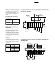
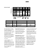
PCB Layout Suggestion
The following PCB layout shows a
recommended layout that should
result in good electrical and EMI
performance. Things to note:
1. The ground plane should be
continuous under the part, but
should not extend under the
shield trace.
2. The shield trace is a wide, low
inductance trace back to the
system ground.
3. The AGND pin is connected to
the ground plane and not to
the shield tab.
4. C1 is an optional V
cc
filter
capacitor; it may be left out if
the V
cc
is clean.
5. VLED can be connected to
either unfiltered or
unregulated power. If C1 is
used, and if VLED is connected
to V
cc
, the connection should
be before the C1 cap.
Component Side
Circuit Side
VLED
TXD
RXD
SHUTDOWN
V
CC
SHIELD
GROUND
C1