
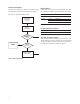
DVD Recorder User Manual

12
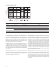
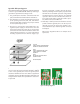
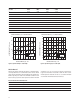
Recommended Metal Solder Stencil Aperture
It is recommended that only a 0.152 mm (0.006 inches)
or a 0.127 mm (0.005 inches) thick stencil be used for
solder paste printing. This is to ensure adequate printed
solder paste volume and no shorting. See the table be-
low the drawing for combinations of metal stencil aper-
ture and metal stencil thickness that should be used.
Aperture opening for shield pad is 2.7 mm x 1.25 mm as
per land pattern.
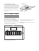
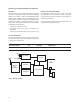
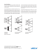
Adjacent Land Keepout and Solder Mask Areas
Adjacent land keep-out is the maximum space oc-
cupied by the unit relative to the land pattern. There
should be no other SMD components within this area.
The minimum solder resist strip width required to avoid
solder bridging adjacent pads is 0.2 mm.
Stencil thickness, Aperture size (mm)
t (mm) length, l width, w
0.152 mm 2.60 ± 0.05 0.55 ± 0.05
0.127 mm 3.00 ± 0.05 0.55 ± 0.05
Figure 14. Solder stencil aperature.
Figure 15. Adjacent land keepout and solder mask areas.
0.2
3.0
10.1
SOLDER MASK
3.85
UNITS: mm
APERTURES AS PER
LAND DIMENSIONS
l
w
t
It is recommended that two ducial crosses be place at
mid-length of the pads for unit alignment.
Note: Wet/Liquid Photo-Imageable solder resist/mask is
recommended.