
DVD Recorder User Manual

2
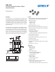
Order Information
Part Number Packaging Type Package Quantity
HSDL-3220-021 Tape and Reel Front View 2500
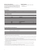
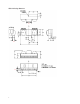
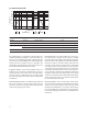
I/O Pins Conguration Table
Pin Symbol Description I/O Type Notes
1 LED A LED Anode I 1
2 LED C LED Cathode 2
3 TXD Transmit Data. Active High. I 3
4 RXD Receive Data. Active Low. O 4
5 SD Shutdown. Active High. I 5
6 Vcc Supply Voltage 6
7 IOVcc Input/Output ASIC Vcc 7
8 GND Ground 8
- Shield EMI Shield 9
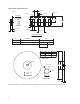
Marking Information
The unit is marked with ‘yyww’ on the shield:
yy = year
ww = work week
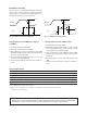
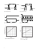
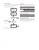
Recommended Application Circuit Components
Component Recommended Value Notes
R1 5.6Ω ± 5%, 0.25 watt for 2.7 ≤Vled< 3.3V
10Ω ± 5%, 0.25 watt for 3.3 ≤Vled<4.2V
15Ω ± 5%, 0.25 watt for 4.2 ≤Vled< 5.5V
CX1, CX4 0.47 µF ± 20%, X7R Ceramic 10
CX2, CX3 6.8 µF ± 20%, Tantalum 11
Notes:
1. Tied through external series resistor, R1, to regulated Vled from 2.7 to 5.5V. Please refer to table above for recommended series resistor value.
2. Internally connected to LED driver. Leave this pin unconnected.
3. This pin is used to transmit serial data when SD pin is low. If this pin is held high for longer than 50 µs, the LED is turned o. Do NOT oat this
pin.
4. This pin is capable of driving a standard CMOS or TTL load. No external pull-up or pull-down resistor is required. The pin is in tri-state when
the transceiver is in shutdown mode. The receiver output echoes transmitted signal.
5. The transceiver is in shutdown mode if this pin is high for more than 400 µs. On falling edge of this signal, the state of the TXD pin sampled
and used to set receiver low bandwidth (TXD=low) or high bandwidth (TXD=high) mode. Refer to the section ”Bandwidth selection timing”
for programming information. Do NOT oat this pin.
6. Regulated, 2.7 to 3.6 Volts.
7. Connect to ASIC logic controller Vcc voltage or supply voltage. The voltage at this pin must be equal to or less than supply voltage.
8. Connect to system ground.
9. Connect to system ground via a low inductance trace. For best performance, do not connect directly to the transceiver pin GND.
10. CX1 must be placed within 0.7 cm of the HSDL-3220 to obtain optimum noise immunity.
11. In environments with noisy power supplies, including CX2, as shown in Figure 1, can enhance supply ripple rejection performance.
Application Support Information
The Application Engineering Group is available to as-
sist you with the application design associated with the
HSDL-3220 infrared transceiver module. You can con-
tact them through your local sales representatives for
additional details.