
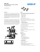
DVD Recorder User Manual

5
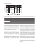
Electrical and Optical Specications
Specications (Min. and Max. values) hold over the recommended operating conditions unless otherwise noted.
Unspecied test conditions may be anywhere in their operating range. All typical values (Typ.) are at 25°C, Vcc set to
3.0V and IOVcc set to 1.8V unless otherwise noted.
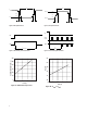
Parameter Symbol Min. Typ. Max. Units Conditions
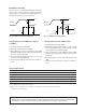
Receiver
Viewing Angle 2θ 30 °
Peak Sensitivity Wavelength λp 880 nm
RXD Output Voltage Logic High V
OH
IOV
CC
– 0.2 IOV
CC
V I
OH
= -200 µA, EI ≤ 0.3
µW/cm
2
Logic Low V
OL
0 0.4 V I
OL
= 200 µA, EI ≥ 8.1 µW/cm
2
RXD Pulse Width (SIR)
[15]
t
PW
(SIR) 1 4.0 µs θ
≤ 15°, C
L
= 9 pF
RXD Pulse Width (MIR)
[16]
t
PW
(MIR) 100 500 ns θ
≤ 15°, C
L
= 9 pF
RXD Pulse Width (FIR)
[16]
t
PW
(FIR) 80 175 ns θ
≤ 15°, C
L
= 9 pF
RXD Rise and Fall Times t
r
, t
f
60 ns C
L
= 9 pF
Receiver Latency Time
[17]
t
L
25 50 µs
Receiver Wake Up Time
[18]
t
W
50 100 µs
Transmitter
Radiant Intensity IE
H
10 45 mW/sr I
LEDA
= 150 mA, θ
≤ 15°, V
TXD
≥ V
IH
,
V
SD
≤ V
IL
, Ta=25°C
Viewing Angle 2θ 30 60 °
Peak Wavelength λ
p
875 nm
Spectral Line Half Width ∆λ 35 nm
TXD Input Current High I
H
10 µA V
TXD
≥ V
IH
Low I
L
10 µA 0 ≤ V
TXD
≤ V
IL
LED ON Current I
LEDA
150 mA V
TXD
≥ V
IH
,
R1=5.6ohm, Vled=3.0V
TXD Pulse Width (SIR) t
PW
(SIR) 1.5 1.6 1.8 µs t
PW
(TXD) = 1.6 µs at 115.2 kbit/s
TXD Pulse Width (MIR) t
PW
(MIR) 148 217 260 ns t
PW
(TXD) = 217 ns at 1.152 Mbit/s
TXD Pulse Width (FIR) t
PW
(FIR) 115 125 135 ns t
PW
(TXD)=125 ns at 4.0 Mbit/s
Maximum Optical PW
[19]
t
PW(max.)
50 100 µs
TXD Rise and fall Time (Optical) t
r
, t
f
600 ns t
PW
(TXD) = 1.4 µs at 115.2 kbit/s
40 ns t
PW
(TXD) = 125 ns at 4.0 Mbit/s
LED Anode On-State Voltage V
ON(LEDA)
1.6 2.1 V I
LEDA
=150 mA, V
TXD
≥V
IH
Transceiver
Supply Current Shutdown I
CC1
0.1 1 µA V
SD
≥ V
IH,
Ta= 25°C
Idle I
CC2
1.8 3.0 mA V
SD
≤ V
IL
, V
TXD
≤ V
IL
, EI=0
Notes:
15. For in-band signals from 9.6 kbit/s to 115.2 kbit/s, where 9 µW/cm
2
≤ EI ≤ 500 mW/cm
2
.
16. For in-band signals from 0.576 Mbit/s to 4.0 Mbit/s, where 22.5 µW/cm
2
≤ EI ≤ 500 mW/cm
2
.
17. Latency time is dened as the time from the last TxD light output pulse until the receiver has recovered full sensitivity.
18. Receiver wake up time is measured from Vcc power on or SD pin high to low transition to a valid RXD output.
19. The maximum optical PW is the maximum time the LED remains on when the TXD is constantly high. This is to prevent long turn on time of
the LED for eye safety protection.