
User's Manual

31 May 2022
3 of 14
RED4S User’s Manuals
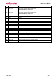
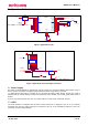
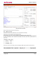
1 Pin Description
17
18
19
VCC36
GND
NC
P01_TXD0
NC
NC
NC
NC
ISP_MODEb
CSE
NC
P15
P16
P17
P12
NC
GND
GND
P00_RXD0
NC
NC
RESETb
SWCLK
SWDIO
GND
GND
GND
GND
GND
GND
VCC36P
VCC36P
20
21
22
23
24
25
26
27
28
29
30
31
32
33
34
35
GND
RFIO
GND
1
2
3
4
5
6
7
8
9
10
11
12
13
15
16
14
Figure 1 Pin Description
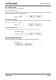
1.1 RED4S Pin Description
No.
Pin Name
Description
1
VCC36
DC Power for Reader SOC
2
GND
Ground
3
P04_SPI_TXD
Quasi-bi directional I/O port or SPI Output
4
P05_SPI_RXD
Quasi-bi directional I/O port or SPI Input
5
P06_SPI_CLK
Quasi-bi directional I/O port or SPI Clock
6
P07_SPI_CS
Quasi-bi directional I/O port or SPI Chip Select
7
ISP_MODEb
When ISP_MODEb is Logic ‘Low’, ISP mode is set as shown below table
Pin No.
7
12
11
10
MODE
ISP_MODEb
P17
P16
P15
Normal
1
GPIO/INT
GPIO/INT
GPIO/INT
UART ISP
0
0
0
0
SPI ISP
0
0
0
1
[CAUTION] Except ISP mode, ISP_MODEb should be set logic ‘High’ for
robust stability for FLASH memory
8
CSE
Chip Select enable / module power enable 0:Disable 1: Enable
9
NC
Not Connection
10
P15
Quasi-bi directional I/O port
[NOTE] This pin is already used internally. So this pin should be only for ISP mode
11
P16
Quasi-bi directional I/O port or External Interrupt 4