
User's Manual


Reproduction forbidden without Fibocom Wireless Inc. written authorization - All Rights Reserved.
FIBOCOM SS808 Series Hardware User Manual Page 35 of 72
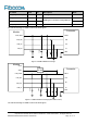
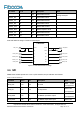
OVP
IN
VDD_3.3V
100nF
Module
USB_VCONN
USB_HS_ID
USB_SS_SWITCH_SEL
OUT
EN
USB_VBUS_IN
B0+
B0-
C0-
C1-
SWITCH
A1-
SEL
B1-
B1+
C0+
C1+
USB_SS_RX_M
VCC
USB_DM
USB_DP
USB_SS_RX_P
USB_SS_TX_P
USB_SS_TX_M
A1+
A0-
A0+
USB_CC2
D-
D+
CC1
CC2
SSTXP1
USB_CC1
Type C Connector
ESD
SSTXN1
SSRXP1
SSRXN1
SSTXP2
SSTXN2
SSRXP2
SSRXN2
VBUS
Figure 12 USB3.0 Reference Design
Note:
1) please chose junction capacitor less than 2pF for ESD protection device of USB_DP/DM
2) USB_DP and USB_DM are high-speed differential signal. The highest transmission rate is 480Mbps.
Please pay attention to the following requirements in PCB layout:
⚫ USB_DP and USB_DM signal cables are required to be parallel and equal in length (differential cable
length controlled within 2mm), while the right-angle route shall be avoided, and differential 90Ω
impedance shall be controlled.
⚫ USB2.0 differential signal cable is laid on the signal layer nearest to the ground, with well grounded
3) USB_ID can be simulated by using GPIO, GPIO_18 by default.
4) Pease choose DC-DC that satisfy output is 5V when support OTG function.
USB3.0 (Type-C) interface circuit design:
1) USB3.0 is a high-speed signal cable and needs to be well-shielded (differential cable ground wrap), and
follows the principle of high-speed differential routing
2) Do differential impedance control, 90 ohms ±10% and control differential cable length within 0.7mm
3) ESD device parasitic capacitor must be less than 0.5pF
3.5 UART
SS808 series module defines three UART ports,all are 1.8V voltage domain. Its pin definition is shown
as follow table:
Table 11 UART Interface Pin Definition