
- PanaXseries_ MICROCOMPUTER MN102H MN102H75K/F75K/85K/F85K LSI User's Manual

General Description
Bus Interface
Panasonic Semiconductor Development Company MN102H75K/F75K/85K/F85K LSI User Manual
36
Panasonic
1.7.2 Bus Interface Control Registers
The external memory wait register (EXWMD) and memory mode register 1
(MEMMD1) control the bus interface.
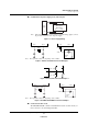
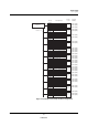
EXWMD: External Memory Wait Register x’00FF80’
EW[33:30], EW[23:20], EW[13:10], EW[03:00]
These fields contain the wait settings for external memory spaces 3, 2, 1,
and 0, respectively. One wait corresponds to one instruction cycle. When
the external oscillator is 4 MHz, one wait is 83 ns.
The OSD, VBI0, VBI1, I2C, IR remote signal receiver, and H counter
blocks apply to external memory space 0.
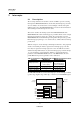
MEMMD1: Memory Mode Register 1 x’00FF82’
Write 0s to bits 15 to 2.
IOW[1:0]: Wait setting for internal I/O space
00: 1 wait
01: Reserved
10: 2 waits
11: 3 waits
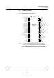
Bit:1514131211109876543210
EW 33 EW 32 EW 31 E W 30 EW 23 EW 22 EW 21 E W 20 EW 13 EW 12 E W 11 EW 10 EW 03 EW 02 EW 01 E W 00
Reset:1110111011101110
R/W: R/WR/WR/WR/WR/WR/WR/WR/WR/WR/WR/WR/WR/WR/WR/WR/W
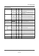
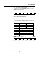
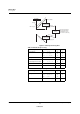
Table 1-4 Wait Count Settings
EW[n3:n0] Setting Wait Count Cycles
0000 0.01.0
0001 R eserved
0010 1.02.0
0011 R eserved
0100 2.03.0
0101 R eserved
0110 3.04.0
0111 R eserved
1000 4.05.0
1001 R eserved
1010 5.06.0
1011 R eserved
1100 6.07.0
1101 R eserved
1110 7.08.0
1111 R eserved
Bit:1514131211109876543210
EB31 EB32 EB21 EB20 EB11 EB10 EB01 EB00 BRS1 BRS0 BRC3 BRC2 BRC1 BRC0 IOW 1 IOW 0
Reset:0000000000000011
R/W: R/WR/WR/WR/WR/WR/WR/WR/WR/WR/WR/WR/WR/WR/WR/WR/W