LS005ONWCS Datasheet IEEE 802.11 1X1 a/b/g/n/ac Wireless LAN Bluetooth 5.2 Combo Stamp Module Datasheet Version 1.
LS005ONWCS Datasheet Date Revision Content Revised By Version 2022/01/25 Initial Release EE V1.0 2022/02/24 Modify BT Specification RF V1.1 Confidential and Proprietary of Luxshare-ict Electronic Technology (KUNSHAN) Ltd.
LS005ONWCS Datasheet Contents 1. Introduction ............................................................................................................................................................. 3 2. Features ................................................................................................................................................................... 4 2.1 Wi-Fi Features .............................................................................................................
LS005ONWCS Datasheet 8.4 Installation Notice to Host Product Manufacturer ...................................................................................... 26 8.5 Antenna Change Notice to Host manufacturer ........................................................................................... 26 8.6 FCC other Parts, Part 15B Compliance Requirements for Host product manufacturer ........................................ 27 8.7 For Class B ..............................................................
LS005ONWCS Datasheet 2. Features 2.1 Wi-Fi Features • • • • • • • • • • • • • Support 802.11 a/b/g/n/ac Dual band: 2.
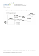
LS005ONWCS Datasheet 3. Block Diagram A simplified block diagram of the LS005ONWCS is depicted in the figure below. Confidential and Proprietary of Luxshare-ict Electronic Technology (KUNSHAN) Ltd.
LS005ONWCS Datasheet 4. Specifications Table 4.1 General Specification Model Name LS005ONWCS Product Description Support Wi-Fi 5/BT 5.2 Functionalities Dimension L x W x H(MAX):15*15*2.55(Max)mm Main Chip 88W8987(NXP) Standard 802.
LS005ONWCS Datasheet 4.2 WLAN&BT Specification 4.2.1 2.4G WLAN Specification Features Operating Frequency Standards Modulation Data Rates Description 2.412GHz~2.472 GHz IEEE 802.11b/g/n, Wi-Fi compliant 802.11b: DQPSK, DBPSK, CCK 802.11g/n: OFDM 802.11b: 1, 2, 5.5, 11Mbps 802.11g: 6, 9, 12, 18, 24, 36, 48, 54Mbps 802.11n: Maximum data rates up to 150Mbps (40MHz channel) 802.11b@11Mbps : 16dBm +/-2dBm @ EVM≦35% 802.11g@54Mbps : 14dBm +/-2dBm @ EVM≦-27dB Output Power 802.
LS005ONWCS Datasheet 4.2.2 5G WLAN Specification Features Description Operating Frequency 5.15GHz~5.825 GHz IEEE 802.11a/n/ac, Wi-Fi compliant Standards Modulation Data Rates 802.11a/n/ac : OFDM 802.11a: 6, 9, 12, 18, 24, 36, 48, 54Mbps 802.11n/802.11ac: Maximum data rates up to 86.7 Mbit/s (20MHz channel), 200 Mbit/s (40MHz channel), 433Mbit/s(80 MHZ channel) 802.11a@54Mbps : 13dBm +/-2dBm @ EVM≦-27dB 802.11n@HT20 MCS 7 : 10dBm +/-2dBm @ EVM≦-28dB 802.
LS005ONWCS Datasheet 4.2.3 BT Specification Standard Modulation Frequency Band Bluetooth 5.2 GFSK, π/4-DQPSK, 8DPSK 2402MHz~2480MHz BDR: typ:2dBm EDR: typ:-1dBm LE: typ:2dBm Output Power BDR(DH1): -86dBm @ BER<0.1% EDR(2DH5): -86dBm @ BER<0.01% LE : -90dBm @ BER<30.8% 79 Channels Sensitivity Number of Channel 4.3 Operating Conditions Operation Conditions VDD33: 3.3V Voltage VIO: 3.3V/1.8V VIO_SD: 1.
LS005ONWCS Datasheet 5. Pin Assignments 5.1 Pin Map LS005ONWCS Top View Pin Map Unit: mm Confidential and Proprietary of Luxshare-ict Electronic Technology (KUNSHAN) Ltd.
LS005ONWCS Datasheet 5.2 Pin Definition Pin No Definition Description Voltage Type 1 GND Ground connections --- --- 2 GND Ground connections --- --- 3 NC No connect to anything --- Floating 1.8V I 1.8V I 10 - SDIO[WLAN] + UART[BT] 11 - SDIO[WLAN] + SDIO[BT] To set a configuration bit to 0, attach a 51k resistor from the pin to ground.
LS005ONWCS Datasheet 22 WL_WAKE_HOST WL device wake-up HOST VIO O 23 GPIO4_PCM_DIN GPIO Mode: GPIO[4] PCM Mode: PCM_DIN VIO I/O I 24 BT_WAKE_HOST Bluetooth device to wake-up HOST VIO O 25 GPIO6_PCM_CLK GPIO Mode: GPIO[6] PCM Mode: PCM_CLK VIO I/O I/O 26 GPIO3 GPIO[3] VIO I/O 27 SD_CMD SDIO Command VIO_SD I/O 28 SD_CLK SDIO Clock input VIO_SD I 29 SD_D0 SDIO Data line 0 VIO_SD I/O 30 SD_D1 SDIO Data line 1 VIO_SD I/O 31 SD_D2 SDIO Data line 2 VIO_SD I/O 32 S
LS005ONWCS Datasheet 5.3 Layout Recommendation Unit: mm Confidential and Proprietary of Luxshare-ict Electronic Technology (KUNSHAN) Ltd.
LS005ONWCS Datasheet 5.4 Physical Dimensions Unit: mm Confidential and Proprietary of Luxshare-ict Electronic Technology (KUNSHAN) Ltd.
LS005ONWCS Datasheet 6. Electrical Characteristics 6.1 Absolute Maximum Ratings Symbol Parameter VDD33 3.3V power supply VIO 1.8V/3.3V digital I/O power supply VIO_SD 1.8V digital SDIO I/O power supply Min Typ Max Units -- 3.3 4.0 V -- 1.8 2.2 V -- 3.3 4.0 V -- 1.8 2.2 V Min Typ Max Units 3.07 3.3 3.53 V 1.67 1.8 1.92 V 3.07 3.3 3.53 V 1.67 1.8 1.92 V 6.2 Recommended Operating Conditions Symbol Parameter VDD33 3.3V power supply VIO 1.8V/3.
LS005ONWCS Datasheet 6.3 DC Characteristics 6.3.1 VIO DC characteristics-3.3V/1.8V operation Symbol Parameter Condition Min Typ Max Units VIH Input high voltage -- 0.7*VIO -- VIOI+0.4 V VIL Input low voltage -- -0.4 -- 0.3*VIO V VHYS Input hysteresis -- 100 -- -- mV VOH Output high voltage -- VIO-0.4 -- -- V VOL Output low voltage -- -- -- 0.4 V 6.3.2 VIO_SD DC characteristics-1.
LS005ONWCS Datasheet 7. Host Interface 7.1 SDIO Interface 7.1.1 Introduction The LS005ONWCS supports a SDIO device interface that conforms to the industry standard SDIO Full-Speed card specification and allows a host controller using the SDIO bus protocol to access the Wireless SoC device. The LS005ONWCS acts as the device on the SDIO bus. The host unit can access registers of the SDIO interface directly and can access shared memory in the device through the use of BARs and a DMA engine.
LS005ONWCS Datasheet 7.1.
LS005ONWCS Datasheet SDIO Timing Data——SDR12, SDR25, SDR50 Modes (up to 100 MHz) Symbol Parameter Condition Min Typ Max Units fPP Clock frequency SDR12/25/50 25 -- 100 MHz TIS Input setup time SDR12/25/50 3 -- -- ns TIH Input hold time SDR12/25/50 0.8 -- -- ns TCLK Clock time SDR12/25/50 10 -- 40 ns SDR12/25/50 -- -- 0.2*TCLK ns SDR12/25/50 -- -- 7.5 ns SDR12/25/50 1.
LS005ONWCS Datasheet TCR,TCF Rise time, fall time TCR,TCF < 0.96 ns (max) at 208 MHz SDR104 -- -- 0.2*TCLK ns SDR104 0 -- 10 ns SDR104 2.88 -- -- ns CCARD = 10 pF TOP TODW Card output phase Output timing of variable data window 7.1.5 SDIO Timing Diagram—DDR50 Mode (50 MHz) SDIO CMD Timing Diagram—DDR50 Mode (50 MHz) SDIO DAT[3:0] Timing Diagram—DDR50 Mode Confidential and Proprietary of Luxshare-ict Electronic Technology (KUNSHAN) Ltd.
LS005ONWCS Datasheet SDIO Timing Data——DDR50 Mode(50MHz) Symbol Parameter Condition Min Typ Max Units Clock time 50 MHz (max) DDR50 20 -- -- ns DDR50 -- -- 0.2*TCLK ns DDR50 45 -- 55 % DDR50 6 -- -- ns DDR50 0.8 -- -- ns DDR50 -- -- 13.7 ns DDR50 1.5 -- -- ns DDR50 3 -- -- ns DDR50 0.8 -- -- ns DDR50 -- -- 7.0 ns DDR50 1.5 -- -- ns Clock TCLK between rising edges TCR,TCF Rise time, fall time TCR,TCF < 4.
LS005ONWCS Datasheet 7.2 UART Host Interface 7.2.1 High-Speed UART Specifications UART Timing Diagram 7.2.2 UART Timing Data Symbol Parameter Condition Min Typ Max Units TBAUD Baud rate 38.4MHz input clk 250 -- -- ns 7.3 PCM Interface 7.3.1 PCM Timing Diagram—Master Mode PCM Timing Specification Diagram for Data Signals—Master Mode Confidential and Proprietary of Luxshare-ict Electronic Technology (KUNSHAN) Ltd.
LS005ONWCS Datasheet PCM Timing Specification Diagram for PCM_SYNC Signal—Master Mode PCM Timing Specification Data—Master Mode Symbol Parameter Condition Min Typ Max Units FBCLK Bit clock frequency -- -- 2/2.048 -- MHz Duty Cycle BCLK Bit clock duty cycle -- 0.4 0.5 0.
LS005ONWCS Datasheet 7.3.2 PCM Timing Diagram—Slave Mode PCM Timing Specification Diagram for Data Signals—Slave Mode PCM Timing Specification Diagram for PCM_SYNC Signal—Slave Mode PCM Timing Specification Data—Slave Mode Symbol Parameter Condition Min Typ Max Units FBCLK Bit clock frequency -- -- 2/2.048 -- MHz Duty CycleBCLK Bit clock duty cycle -- 0.4 0.5 0.
LS005ONWCS Datasheet TDIHO TBFSU TBFHO Hold time for PCM_DIN after -- 10 -- -- ns -- 15 -- -- ns -- 10 -- -- ns PCM_CLK falling edge Setup time for PCM_SYNC before PCM_CLK falling edge Hold time for PCM_SYNC after PCM_CLK falling edge 8. FCC Statement: Please take attention that changes or modification not expressly approved by the party responsible for compliance could void the user’s authority to operate the equipment. This device complies with Part 15 of the FCC Rules.
LS005ONWCS Datasheet 8.2 Antenna used BT BLE 2.4G Wi-Fi 5G Wi-Fi Antenna Type Max. Antenna Gain PCB Antenna PCB Antenna PCB Antenna PCB Antenna 3.21dBi 3.21dBi 3.21dBi U-NII-1: 3.35dBi U-NII-2A: 3.71dBi U-NII-2C: 3.83dBi U-NII-3: 3.08dBi 8.
LS005ONWCS Datasheet 8.6 FCC other Parts, Part 15B Compliance Requirements for Host product manufacturer This modular transmitter is only FCC authorized for the specific rule parts listed on our grant, host product manufacturer is responsible for compliance to any other FCC rules that apply to the host not covered by the modular transmitter grant of certification.