
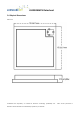
Data Sheet


Confidential and Proprietary of Luxshare-ict Electronic Technology (KUNSHAN) Ltd. , which are not permitted to
disclose to others and shall not be distributed, reproduced, or disclosed
LS005ONWCS
Datasheet
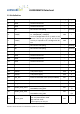
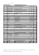
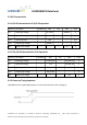
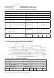
7.1.2 SDIO Interface Signals
Pin Name Type Description
SD_CMD I/O
SDIO 4-bit Mode: Command line
SDIO 1-bit Mode: Command line
SD_CLK I
SDIO 4-bit Mode: Clock
SDIO 1-bit Mode: Clock
SD_D0 I/O
SDIO 4-bit Mode: Data line Bit[0]
SDIO 1-bit Mode: Data line
SD_D1 I/O
SDIO 4-bit Mode: Data line Bit[1]
SDIO 1-bit Mode: Interrupt
SD_D2 I/O
SDIO 4-bit Mode: Data line Bit[2] or read wait (optional)
SDIO 1-bit Mode: Read wait (optional)
SD_D3 I/O
SDIO 4-bit Mode: Data line Bit[3]
SDIO 1-bit Mode: Not used
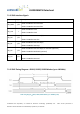
7.1.3 SDIO Timing Diagram—SDR12, SDR25, SDR50 Modes (up to 100 MHz)
SDIO Timing Diagram—SDR12, SDR25, SDR50 Modes (up to 100 MHz) (1.8V)