
Data Sheet


Confidential and Proprietary of Luxshare-ict Electronic Technology (KUNSHAN) Ltd. , which are not permitted to
disclose to others and shall not be distributed, reproduced, or disclosed
LS005ONWCS
Datasheet
Contents
1. Introduction ............................................................................................................................................................. 3
2. Features ................................................................................................................................................................... 4
2.1 Wi-Fi Features ................................................................................................................................................ 4
2.2 Bluetooth Features ........................................................................................................................................ 4
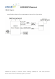
3. Block Diagram .......................................................................................................................................................... 5
4. Specifications Table .................................................................................................................................................. 6
4.1 General Specification ..................................................................................................................................... 6
4.2 WLAN&BT Specification ................................................................................................................................. 7
4.2.1 2.4G WLAN Specification .................................................................................................................... 7
4.2.2 5G WLAN Specification ....................................................................................................................... 8
4.2.3 BT Specification ................................................................................................................................... 9
4.3 Operating Conditions ..................................................................................................................................... 9
5. Pin Assignments ..................................................................................................................................................... 10
5.1 Pin Map ........................................................................................................................................................ 10
5.2 Pin Definition ............................................................................................................................................... 11
5.3 Layout Recommendation ............................................................................................................................. 13
5.4 Physical Dimensions ..................................................................................................................................... 14
6. Electrical Characteristics ........................................................................................................................................ 15
6.1 Absolute Maximum Ratings ......................................................................................................................... 15
6.2 Recommended Operating Conditions .......................................................................................................... 15
6.3 DC Characteristics ........................................................................................................................................ 16
6.3.1 VIO DC characteristics-3.3V/1.8V operation ..................................................................................... 16
6.3.2 VIO_SD DC characteristics-1.8V operation ....................................................................................... 16
6.3.3 Power up Timing Sequence .............................................................................................................. 16
7. Host Interface ........................................................................................................................................................ 17
7.1 SDIO Interface .............................................................................................................................................. 17
7.1.1 Introduction ...................................................................................................................................... 17
7.1.2 SDIO Interface Signals ....................................................................................................................... 18
7.1.3 SDIO Timing Diagram—SDR12, SDR25, SDR50 Modes (up to 100 MHz) .......................................... 18
7.1.4 SDIO Timing Diagram—SDR104 mode (208MHz) ............................................................................. 19
7.1.5 SDIO Timing Diagram—DDR50 Mode (50 MHz) ............................................................................... 20
7.2 UART Host Interface ..................................................................................................................................... 22
7.2.1 High-Speed UART Specifications ....................................................................................................... 22
7.2.2 UART Timing Data ............................................................................................................................. 22
7.3 PCM Interface .............................................................................................................................................. 22
7.3.1 PCM Timing Diagram—Master Mode ............................................................................................... 22
7.3.2 PCM Timing Diagram—Slave Mode .................................................................................................. 24
8. FCC Statement: ...................................................................................................................................................... 25
8.1 Operational use conditions .......................................................................................................................... 25
8.2 Antenna used ............................................................................................................................................... 26
8.3 Labelling Instruction for Host Product Integrator ........................................................................................ 26