
User's Manual


R3-NMW1F
5-2-55, Minamitsumori, Nishinari-ku, Osaka 557-0063 JAPAN
Phone: +81(6)6659-8201 Fax: +81(6)6659-8510 E-mail: info@m-system.co.jp
EM-8286 P. 8 / 10
MODBUS I/O ASSIGNMENTS
ADDRESS DATA FORMAT NAME
Coil (0X) 1 – 1024 Digital Output (discrete output)
1025 Main / Sub Switching Command (valid only with SW3-3 set to ON)
Inputs (1X) 1 – 1024 Digital Input (discrete input)
1025 – 1040 Module Status
1041 – 1056 Error Status
1057 – 1072 Data Error Status
Input Registers (3X) 1 – 256 I Analog Input
257 – 768 F Analog Input
Holding Registers (4X) 1 – 256 I Analog Output
257 – 768 F Analog Output
I: Integer, 0 – 10000 (0 – 100%)
F: Floating (32-bit data cannot be accessed using floating addresses.)
Note: DO NOT access addresses other than mentioned above. Such access may cause problems such as inadequate operation.
• Module Status indicates whether individual I/O modules are mounted or not. The bit corresponding to the mounted slot
turns to “1,” and the unmounted slot to “0.”
• Error Status indicates error status for each module as described below. The bit corresponding to such module turns to “1.”
R3-TSx, R3-RSx, R3-US4: Input burnout
R3-DA16A: Power input in error or disconnected
R3-YSx: Output current error (e.g. load unconnected)
• Data Error Status indicates overrange (R3-US4: out of -10% to +110%; the other types: out of -15% to +115%) status for each
module. The bit corresponding to such module turns to “1.”
• Main / Sub Switching Commands given to the network modules result as follows:
‘MAIN’ MODULE ‘SUB’ MODULE OUTPUT MODE
1 0 Main bus is used; Red LED turns on at RUN LED of the I/O modules.
0 1 Sub bus is used; Green LED turns on at RUN LED of the I/O modules.
1 1 Main bus is used; Amber LED turns on at RUN LED of the I/O modules.
0 0 Output is invalid; RUN LED of the I/O modules turns off.
• Writing to Coil (0X) and Holding Registers (4X) is only available with either Wireless or Modbus communication. It is
available to change the configuration with Configurator Software (model: R3CON). Factory default setting is Modbus com-
munication.
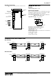
TRANSMISSION DATA ASSIGNMENTS
DIP SW located at the side of the module specifies each I/O module’s data allocation (occupied data area).
For example, when the data areas are assigned as shown below:
Module 1 4
Module 2 4
Module 3 4
Module 4 1
Module 5 1
Module 6 1
Module 7 1
Then the I/O data are assigned as in the table below:
ADDRESS POSITION ADDRESS POSITION
Input Registers (3X)
Holding Registers (4X)
1 – 4, 257 – 264 Slot 1 Coil (0X)
Inputs (1X)
1 – 64 Slot 1
5 – 8, 265 – 272 Slot 2 65 – 128 Slot 2
9 – 12, 273 – 280 Slot 3 129 – 192 Slot 3
13, 281 – 282 Slot 4 193 – 208 Slot 4
14, 283 – 284 Slot 5 209 – 224 Slot 5
15, 285 – 286 Slot 6 225 – 240 Slot 6
16, 287 – 288 Slot 7 241 – 256 Slot 7
For Coil (0X) and Inputs (1X), addresses 16 times assigned
data areas (Data Allocation Type) are allotted with the Data
Allocation Type ‘1’ and ‘4.’ With ‘8’ and ‘16,’ 64 (4 × 16) are
automatically allotted.