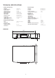
Service Manual CD5004 /N1B/N1SG U1B/K1SG/K1B CD Player CD PLAYER CD5004 MP3/WMA STANDBY DISPLAY OFF PHONES CD5004 ON/STANDBY LEVEL - + • For purposes of improvement, specifications and design are subject to change without notice. • Please use this service manual with referring to the operating instructions without fail. • Some illustrations using in this service manual are slightly different from the actual set. CD5004 S0055V01DM/DG1006 Copyright 2010 D&M Holdings Inc. All rights reserved.
MARANTZ DESIGN AND SERVICE Using superior design and selected high grade components, MARANTZ company has created the ultimate in stereo sound. Only original MARANTZ parts can insure that your MARANTZ product will continue to perform to the specifications for which it is famous. Parts for your MARANTZ equipment are generally available to our National Marantz Subsidiary or Agent. ORDERING PARTS : Parts can be ordered either by mail or by Fax.. In both cases, the correct part number has to be specified.
SAFETY PRECAUTIONS The following check should be performed for the continued protection of the customer and service technician. LEAKAGE CURRENT CHECK Before returning the unit to the customer, make sure you make either (1) a leakage current check or (2) a line to chassis resistance check. if the leakage current exceeds 0.5 milliamps, or if the resistance from chassis to either side of the power cord is less than 460 kohms, the unit is defective.
NOTE FOR SCHEMATIC DIAGRAM WARNING: Parts marked with this symbol z have critical characteristics. Use ONLY replacement parts recommended by the manufacturer. CAUTION: Before returning the unit to the customer, make sure you make either (1) a leakage current check or (2) a line to chassis resistance check. If the leakage current exceeds 0.5 milliamps, or if the resistance from chassis to either side of the power cord is less than 460 kohms, the unit is defective.
WARNING AND LASER SAFETY INSTRUCTIONS GB WARNING NL All ICs and many other semi-conductors are susceptible to electrostatic discharges (ESD). Careless handling during repair can reduce life drastically. When repairing, make sure that you are connected with the same potential as the mass of the set via a wrist wrap with resistance. Keep components and tools also at this potential. F WAARSCHUWING Alle IC’s en vele andere halfgeleiders zijn gevoelig voor elektrostatische ontladingen (ESD).
TECHNICAL SPECIFICATIONS nn Audio characteristics • • • • • • • • • Channels: Frequency response: Dynamic range: Signal-to-noise ratio: Channel separation: Harmonic distortion: Wow & flutter: Audio output: Headphone output: • Digital output Coaxial output (pin jack): Optical output (square optical connector): nn Power supply • • • • • 2 channels 2 Hz to 20 kHz 100 dB 110 dB 110 dB (1 kHz) 0.002% (1 kHz) Precision of quartz 2.25 V rms, stereo 18 mW/32 ohms (variable maximum) nn Cabinet, etc.
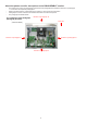
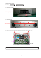
DISASSEMBLY • Disassemble in order of the arrow of the figure of following flow. • In the case of the re-assembling, assemble it in order of the reverse of the following flow. • In the case of the re-assembling, observe "attention of assembling" it. • I f wire bundles are untied or moved to perform adjustment or parts replacement etc., be sure to rearrange them neatly as they were originally bundled or placed afterward. Otherwise, incorrect arrangement can be a cause of noise generation.
About the photos used for descriptions in the DISASSEMBLY" section. • The direction from which the photographs used herein were photographed is indicated at "Direction of photograph: ***" at the left of the respective photographs. • Refer to the table below for a description of the direction in which the photos were taken. • Photographs for which no direction is indicated were taken from above the product. • The photograph is CD5004 K1SG.
1. FRONT PANEL ASSY Proceeding : TOP COVER → FRONT PANEL ASSY (1) Remove the Loadr Panel. Direction of photograph: B (2) Remove the screws. View from bottom (3) Disconnect the connector wire and FFC Cable. Remove the screws. Cut the wire clamp bands. cut CN81 FFC Cable Please refer to "EXPLODED VIEW" for the disassembly method of each P.W.B included in FRONT PANEL ASSY.
2. MAIN PWB Proceeding : TOP COVER → MAIN PWB (1) Remove the screws. Direction of photograph: A (2) Remove the screws. Disconnect the connectors wire and FFC Cable.
3. POWER PWB Proceeding : TOP COVER → POWER PWB (1) Remove the screws. Direction of photograph: A (2) Remove the screws. Disconnect the connector wires. Cut the wire clamp band.
4. AUDIO PWB Proceeding : TOP COVER → AUDIO PWB (1) Remove the screws. Direction of photograph: A (2) Remove the screws. Disconnect the connector wires.
5. MECHA ASSY Proceeding : TOP COVER → FRONT PANEL ASSY → MECHA ASSY (1) Remove the screws. MECHA ASSY (2) Solder the short-circuit before disconnect the FFC Cable. Short (3) Disconnect the connectors wire and FFC Cable. Cut the wire clamp bands.
REMOVING DISCS (1) Remove the Top Cover. (2) Remove the screws. (3) Remove the disc clamper.
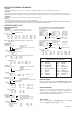
SERVICE MODE AND TAKING THE DISC OUT OF EMERGENCY [A] SERVICE MODE (1) Insert mains cable plug in the outlet. (The Unit is standby mode.) (2) P ress the button While pressing 7/9 and 2 Button. Model name is displayed. CD5004 (3) P ress 7/9 button. Version of microprocessor is displayed. 2008-05-16-1 (4) P ress 7/9 button. Light up all FL segment.
HOW TO THE RESET OF PLAYBACK TIME When replacing CD MECHANISM (TRAVERSE), please reset Playback time (total) in the following procedure. (1) Procedure 6 of SERVICE MODE, Playback time (total) is displayed. PTime : 00051h The display is a time unit. (Example: "10050 hours, 0 minute, 1 second " is 10051h) The maximum Playback time is 65536h. (2) P ress 2 Button 3 seconds and more. PTime Clear? is displayed. PTime Clear? (3) P ress 1 Button. Done is displayed after PTime:00000h is displayed.
VERSION UPGRADE PROCEDURE OF FIRMWARE ABOUT REPLACE THE MICROPROCESSOR WITH A NEW ONE When replaced of the U-PRO (Microprocessor) or the Flash ROM, confirm contents of the following. PWB Name Ref. No. MAIN IC21 After replaced Description Remark B T5CD2(F AAD JZ) CD5004 After replaced A : Mask ROM (With software). No need write-in of software to the microprocessor. B : Flash ROM (With software). Usually, no need write-in of software.
(3) Double click FlashProg.exe, and launch the Flash Programmer. NOTE : W hen a Flash Programmer does not launch even if double-clicked FlashProg.exe, please refer to "2. When a Flash Programmer did not launch". (4) Click OK. NOTE : S ince Flash Programmer communicates with the unit automatically, the following dialog box appears when it fails in communication.
(5) Click the Setup in the menu bar and select the Object file. (6) Click Browse.
(7) Choose the Motorola S Format(*.s16,*.s24,*.s32) in Files of type. Choose the CD5004_yymmdd_x.s24, and click Open. NOTE : The yy is two digits of year. The mm is month. The dd is date. The x is release number. CD5004_yymmdd_x.s24 CD5004_yymmdd_x.s24 (8) Click Device tab.
(9) Choose the TMP91FW60 in the Device, and choose the 900/L1 in the Series. And click Communication tab. (10) Choose the Serial port number in the COM Port. Check the Data Rate Manual, and choose the 38400 in the Data Rare. And Click OK.
(11) Disconnect the mains cord from the unit. (12) Connect the RS-232C on the connection JIG and the Serial Port of windows PC with RS-232C cable. (13) Connect FFC (upside contact) to the rear panel of the unit from connection JIG. (14) Connect the mains cord into the unit. (15) If the connection with the Flash Programmer is successfully made, a dialogue box saying "Erase All data in this devise? (Y/N)" appears automatically. If the connection fails, error message will appear. (Ex.: E000) Click Yes.
(17) Click P (Program) to start update. (18) Software is written into the microprocessor. The writing of software takes about 50 seconds. (19) If the software is updated successfully, a dialog box saying "R006: Programming completed successfully." appears. Click OK.
(20) Click the File in the menu bar and select the Exit. (21) Disconnect mains cord from the unit, and then disconnect FFC of connection JIG from the unit. 2. When a Flash Programmer did not launch (1) Open the FlashProg.ini in the Flash Programmer folder by text editor. (EX.
(2) Delete the text "OpenFile=C:\...(your PC setting)...\???.s24".
(3) Save the FlashProg.ini. (4) Close the text editor. (5) Probably you can launch the Flash Programmer. Go to the 1. Update Procedure step 3.
TROUBLE SHOOTING 1. POWER PWB N.G. Check FUSE Condition ・FUSE [F901]OPEN? (Open) Check the output short of trans ([T901][T902]). If trans is short, trans is replaced. O.K. Check ST+5V output ・Voltage Check +5V DC (switched) Voltage is O.K.? ・[BN45] 5pin output N.G. Check [Q902]corrector input voltage. Check Parts and Soldering and Other Circuits. If abnormality is not found, [Q902] is replaced. N.G. Check the control signal for relay drive. TRANS_ON/OFF signal : 5V ・[BN45] 11pin O.K.
2. FRONT PWB 2.1. FL TUBE dosen't light Check the power supply voltage. Check the VP (+36V)output. +36V DC (switched) Voltage is O.K.? ・[CN21] 19pin N.G. POWER PWB ・[Q901] input Check Parts and Soldering and Other Circuits. If abnormality is not found, [Q901] is replaced. O.K. Check the power supply voltage. Check the VDD(+5V) output. +5V DC (switched) Voltage is O.K.? ・[CN21] 18pin N.G. POWER PWB ・[IC92] 1pin input Check Parts and Soldering and Other Circuits.
3. AUDIO PWB 3.1 No Audio output Check the analog signal output. ・[IC75] 14pin,15pin,18pin,19pin O.K. Check the mute signal (-12V). AUDIO PWB ・[Q603][Q703] base O.K. AUDIO PWB ・[Q605][Q606][Q705][Q706] and Circumference Replace the abnormal IC. N.G. Check the power supply voltage. ・[IC76] 2pin (3.3V) ・[IC77] 3pin (5V) N.G. POWER PWB ・[IC94] AUDIO PWB ・[IC76][IC77] Check Parts and Soldering and Other Circuits. Replace the abnormal output IC. O.K. Check the digital signal input.
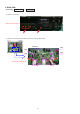
MEASURING METHOD AND WAVEFORMS Measuring Disc: 4822 397 30184 TCD-784 (It is better to use wires for extending between the probe and test points.) 1.
2. WAVEFORMS 1. DISC PLAY RF WAVEFORM(EYE-PATTERN) 2. DISC DETECTION 1.1 CD(TCD-784)Play 2.1 CD(TCD-784)DISC DETECTION 1V 200mV RF FE Focus 2V TE Tracking SLID SPIN 500Mv 2V 1V 2V 2.2 CD-R(TCD-R000RM)DISC DETECT 1.2 CD-R(TCD-R000RM)Play RF FE Focus TE Tracking SLID SPIN 1V 200mV 2V 500Mv 2V 1V 2V 2.3 CD-RW(TCD-W000RM)DISC DETECTION 1.
3. TOC READ 4. FOCUS ADJUSTMENT 3.1 CD(TCD-784)TOC READ 4.1 CD(TCD-784)FOCUS ADJUSTMENT RF FE 1V 200mV Focus 2V TE Tracking 500Mv SLID SPIN 2V 1V 2V 3.2 CD-R(TCD-R000RM)TOC READ RF FE 4.2 CD-R(TCD-R000RM)FOCUS ADJUSTMENT 1V 200mV Focus 2V TE Tracking 500Mv SLID SPIN 2V 1V 2V 3.3 CD-RW(TCD-W000RM)TOC READ 4.3 CD-R(TCD-R000RM)FOCUS ADJUSTMENT 1V 200mV RF FE Focus 2V TE Tracking 500Mv 2V 1V 2V SLID SPIN 5.
I2C (SBI1) W B D H A C E L IX 1Y IZ SP 5 6 44~ 9~ MODE CONTROLLER CE1 DATA BUS 53 ADDRESS BUS 54 8bit TIMER (TMRA3) 55 Clock Timer 41 CD-CCE 43 PORT CD-RST 38 RST 4 VDD 5 VSS 2 24-Bit DSP 3 VDD FOO TRO FMO DMO MT-STBY OP-M CL-M LIMIT-SW CL-SW OP-SW SPINDLE MOTOR M RL3 92 MDI 91 LDO SLED+ M SLED MOTOR SLED- TR+/- SPINDLERL1 SPINDLE+ SLED- Peripheral I/F 1 Mbit SRAM SLED+ RL2 +VREF +8V PLL/VCO D A B 1.5V F +RF3.3V +VREF 62 63 64 +VREF 3.3VDA +3.3V +P1.
POWER SUPPLY BLOCK DIAGRAM AC INLET STANDBY TRANS (T902) (Q902) +5V U-CON (IC21) IR (RS51) REMOTE IN/OUT MAIN RELAY (RY91) ← STANDBY ON/OFF RELAY MAIN TRANS (T901) (IC77) (IC76) +5V +3.3V (IC94) +12V AUDIO HEAD PHONE -12V RELAY (IC93) (IC92) (IC91) +8V SERVO DRIVE MECHA DRIVE +5V RELAY (IC33) (IC25) +3.3V +1.8V (IC34) CD DSP PITCH CONTROL +1.
WIRING DIAGRAM AC B TYPE 7P INLET BK91 L BLACK BK21 SW41 CN22 CN23 (UPDATE PORT) RED JK43 JK42 JK71 JK61 FLASHER PWB CN41 BN41 SUB TRANS CORE BK75 JK41 N CORE CN43 BN43 DSP N BN45 MCU CN45 CN91 AUDIO PWB RELAY MAIN PWB CN44 CN92 CN42 CN21 N CN31 CN33 POWER PWB B TYPE CN32 CORE 16P BN42 BN44 CN81 CN94 CN93 TRANSF.
PRINTED WIRING BOARDS MAIN (COMPONENT SIDE) 1 2 3 4 5 6 7 8 9 A B C D E F G 鉛フリー半田 半田付けには、鉛フリー半田 (Sn-Ag-Cu) を使用してください。 Lead-free Solder When soldering, use the Lead-free Solder (Sn-Ag-Cu).
MAIN (FOIL SIDE) 9 8 7 6 5 4 3 2 1 A B C D E F G 鉛フリー半田 半田付けには、鉛フリー半田 (Sn-Ag-Cu) を使用してください。 Lead-free Solder When soldering, use the Lead-free Solder (Sn-Ag-Cu).
FRONT (COMPONENT SIDE) 1 2 TACT SW (COMPONENT SIDE) 3 4 5 6 7 8 9 10 11 12 1 2 3 A A B B C C D FRONT (FOIL SIDE) 12 11 TACT SW (FOIL SIDE) 10 9 8 7 6 5 4 3 2 1 3 半田付けには、鉛フリー半田 (Sn-Ag-Cu) を使用してください。 Lead-free Solder When soldering, use the Lead-free Solder (Sn-Ag-Cu).
AUDIO (COMPONENT SIDE) 1 2 AUDIO (FOIL SIDE) 3 4 5 6 7 7 6 5 4 3 2 1 A A B B C C D D E E F F G G H H I I 鉛フリー半田 半田付けには、鉛フリー半田 (Sn-Ag-Cu) を使用してください。 Lead-free Solder When soldering, use the Lead-free Solder (Sn-Ag-Cu).
POWER (COMPONENT SIDE) 12 13 POWER (FOIL SIDE) 14 15 16 17 18 7 6 5 4 3 2 1 A A B B C C D D E E F F G G H H 鉛フリー半田 半田付けには、鉛フリー半田 (Sn-Ag-Cu) を使用してください。 Lead-free Solder When soldering, use the Lead-free Solder (Sn-Ag-Cu).
HEADPHONE (COMPONENT SIDE) 1 2 3 FLASHER (COMPONENT SIDE) 4 1 5 2 FLASHER (FOIL SIDE) 3 4 4 3 2 1 A A A B B B C C C D E F TRANSF (COMPONENT SIDE) TRANSF (FOIL SIDE) 5 4 3 4 1 A HEADPHONE (FOIL SIDE) 5 2 3 2 1 A B B C C D D 鉛フリー半田 半田付けには、鉛フリー半田 (Sn-Ag-Cu) を使用してください。 E Lead-free Solder When soldering, use the Lead-free Solder (Sn-Ag-Cu).
5 6 CD-OPEN-M 0.015u 1 2 3 4 5 6 5 1 2 3 A PDIC A D PDIC D E PDIC E 5 PDIC VC C326 100/16V +VREF DAGND DAGND 16 15 PDIC VCC 3.3VDA DAGND DAGND L401 VDD 47P 10 R403 3 220 R401 DGND DGND 2 TX 47/25V 1 DGND JK42 0 COAXIAL OUT 0 C409 0.1uF(NC) R412 DGND DGND DGND DGND DGND ST+5V 47K C410 SW41 DGND DGND 1SS355T D401 R416 47K D R418 47 C411 C412 0.1uF 0.
1 2 3 4 5 6 7 8 R606 750 1500P 33 R614 L CHANNEL JK61 R622 R623 47 68 R621 GND 4.7K 4.7K C613 R619 Q606 KTC2874 470K Q605 KTC2874 GND 3.9K 47K R616 R628 47K(N.C) 33 R615 33 R612 C616 100P(FILM) GND GND GND 100P(N.C) C611 3.9K 220/16V 68 GND GND -12V 3.9K GND KTA1268 Q702 GND 47 R719 R721 4.7K 4.7K C713 R723 68 Q706 KTC2874 GND D707 1.2K 1.2K R624 R724 GND 100P(N.C) R722 470K R716 R728 47K(N.C) 33 R715 47K Q705 KTC2874 33 R712 2.
EXPLODED VIEW 38 NO. PARTS NO. DESCRIPTION Q'TY A/S PART S1 CTB3+6JR S2 CTB3+6FFB S3 CTBD3+8JFB SCREW 12 O.K SCREW 4 O.K SCREW , DOT 1 O.K S4 CTB3+8JFB S5 CTW3+8JR S6 CTW3+8JFZR SCREW 18 O.K SCREW 6 O.K SCREW 6 O.K S7 CTB3+10JR S8 CTB3+10JFB S9 CTW3+12JR SCREW 12 O.K SCREW 5 O.K SCREW 4 O.K S10 CTW3+18JR S11 CTB4+6FR SCREW 2 O.K SCREW 2 O.
PARTS LIST OF EXPLODED VIEW * Parts for which "nsp" is indicated on this table cannot be supplied. * P.W.B. ASS'Y for which "nsp" is indicated on this table cannot be supplied. When repairing the P.W.B. ASS'Y, check the board parts table and order replacement parts. * The parts listed below are for maintenance only, might differ from the parts used in the unit in appearances or dimensions. Note: The symbols in the column "Remarks" indicate the following destinations. Ref. No.
Ref. No. Part No.
PACKING VIEW r Q3 e w z Q4 Q5 q e Q8 Q7 Q6 Q9 Q8 Q7 PARTS LIST OF PACKING VIEW * Parts for which "nsp" is indicated on this table cannot be supplied. * The parts listed below are for maintenance only, might differ from the parts used in the unit in appearances or dimensions. Note: The symbols in the column "Remarks" indicate the following destinations. Ref. No. U : North America model B : Black model N : Europe model SG : Silver Gold model Part No.
SEMICONDUCTORS T5CD2 Only major semiconductors are shown, general semiconductors etc. are omitted to list. The semiconductor which described a detailed drawing in a schematic diagram are omitted to list. 1. IC's 1.
Terminal Function Pin Port Name No.
Pin Port Name No.
IS61C256AL (MAIN : IC23) TC7WHU04FU (MAIN : IC26) 51
CDCE913 CDCEL913 www.ti.com CDCE913PWR (MAIN: IC27) SCAS849B – JUNE 2007 – REVISED DECEMBER 2007 Programmable 1-PLL VCXO Clock Synthesizer With 1.8-V, 2.5-V, and 3.3-V Outputs FEATURES • Flexible Clock Driver • Member of Programmable Clock Generator – Three User-Definable Control Inputs Family [S0/S1/S2], for example., SSC Selection, CDCE913 Frequency Switching, Output Enable, or – CDCE913/CDCEL913: 1-PLL, 3 Outputs CDCEL913 Power Down www.ti.
TC94A70FG/TC94A73MFG Single-chip CD-MP3 Processor TC94A70FG (MAIN : IC31) TC94A70FG Description and audio DSP ware library MP3, WMA, CD, AAC, graphic ion, and popular sound formats atibility between c TC94A70FG em-in-package 94A73MFG with DRAM enables a rdware design to tandard and c shock protection D playback 75 74 73 72 71 70 69 68 67 66 65 64 63 62 61 60 59 58 57 56 55 54 53 52 51 LDo 91 electronic MDi 92 shock protection (ESP) with 93 RVSS3firmware DSP and 16 Mbit DRAM in an FNi2 94
TC94A70FG TC94A70FG 1. Pin Descriptions Terminal Function Pin No. Symbol 1 AVSS3 2 RFZi 3 RFRP 4 SBAD/RFDC 5 FEi 6 TEi 7 TEZi 8 AVDD3 9 10 Foo TRo 11 VREF 12 FMo 13 DMo 14 VSSP3 15 VCOi 16 VDDP3 17 18 VDD1 VSS 19 FGiN 20 io0(/HSo) 21 io1(/UHSo) 22 XVSS3 I/O Description Default - I 3AI/F O 3AI/F Grounding pin for 3.3V CD analog circuits.
5 V regulator reference amp (with external output Tr.) Thermal shut down protection Operating supply voltage range: VCC = 5.0-9.0 V Block Diagram TA2125AF (MAIN : IC32) Block Diagram 4ch Driver REG RIN FIN STB IN3 IN4 STB VR VCC RL4 REG OUT 36 35 34 Control Logic 33 32 31 30 29 28 2 3 4 27 26 25 24 5 6 7 8 N.C. N.C. RL5 23 22 3 STBY STBY Iref 1 FIN 9 TSD FIN 21 11 GND 12 13 14 20 19 3 3 3 3 10 RL3 N.C.
TC74HCU04AFNG (FRONT: IC51) 56
D/A, Output Analog Filtering digital-to-analog conversion, digital de-emphasis, volz 114 dB Dynamic Range ume control, channel mixing and analog filtering. The z 100 dB THD+N advantages of this architecture include: ideal differential CS4392 linearity, no distortion mechanisms due to resistor z Up to 192kHz Sample Rates matching errors, no linearity drift over time and temperaz Direct Stream Digital Mode CS4392KZZ (AUDIO: IC75) ture, and a high tolerance to clock jitter. z Low Clock Jitter Sensitivity 1.
PARTS LIST OF P.W.B. UNIT * Parts for which "nsp" is indicated on this table cannot be supplied. * The parts listed below are for maintenance only, might differ from the parts used in the unit in appearances or dimensions. Note: The symbols in the column "Remarks" indicate the following destinations. U : North America model N : Europe model K : China model AUDIO PWB (CUP12097Z-2) Ref. No. Part No.
Ref. No. C754 C755 C756 C757 C758 C759 C760 C761 C790 C791 Part No. 00MOA10701620 00MOA22605020 nsp 00MOA22605020 00MOA47602520 nsp nsp 00MOA22702520 nsp nsp OTHERS PARTS GROUP BK75 nsp BN42 nsp BN43 nsp Part Name Remarks Q'ty New ELECT CAP100UF 16V ELECT CAP22UF 50V CER. CAP0.1UF 50V Z CERAMIC ELECT CAP22UF 50V ELECT CAP47UF 25V CER. CAP0.1UF 50V Z CERAMIC CER. CAP0.1UF 50V Z CERAMIC ELECT CAP220UF 25V CER. CAP0.1UF 50V Z CERAMIC CER. CAP0.
FRONT PWB (CUP12097Z-1) Ref. No. Part No. SEMICONDUCTORS GROUP IC51 90M-HC700550R Part Name Remarks Q'ty New IC TC74HCU04AFNG HVI74HCU04AFNG Q502 Q503 90M-BA001460R 90M BA001460R TRS KRC107M TRS KRC107M HVTKRC107MT HVTKRC107MT D502 D503 90M-HI101120R 90M-HI101120R L.E.D SLR325VRA47 L.E.D SLR325VRA47 KVDSLR325VRA47 KVDSLR325VRA47 FL51 90M-HQ300610R FL DISPLAY FOR CD5400 CFLHCA12SS18T CAPACITORS GROUP C501 nsp C502 nsp C503 00MEJ47601640 C504 00MEJ47601640 C505 nsp CER. CAP0.
HEADPHONE PWB (CUP12097Z-4) Ref. No. Part No.
MAIN PWB (CUP12096Z) Ref. No. Part No.
Ref. No. C301 C306 C310 C311 C312 C313 C314 C315 C316 C317 C318 C319 C320 C321 C322 C323 C324 C325 C326 C327 C328 C329 C330 C331 C332 C333 C334 C335 C336 C337 C338 C339 C340 C341 C342 C343 C344 C345 C346 C347 C348 C349 C350 C351 C352 C353 C354 C360 C361 C362 C363 C364 C365 C401 C402 C403 C404 C405 C406 C408 C410 C411 C412 C431 C433 C461 C462 Part No.
Ref. No. C465 C466 C467 C468 C990 C991 Part No. 00MDK96104300 00MOA10701620 00MOA10701620 00MDK96104300 00MDK96104300 00MDK96104300 OTHERS PARTS GROUP BK21 nsp BK31 nsp Part Name Remarks Q'ty New CER. CAP.0.1UF 50V K ELECT CAP.100UF 16V ELECT CAP.100UF 16V CER. CAP.0.1UF 50V K CER. CAP.0.1UF 50V K CER. CAP.0.1UF 50V K CCUS1H104KC CCEA1CH101T CCEA1CH101T CCUS1H104KC CCUS1H104KC CCUS1H104KC BRACKET FOR PWB HEAT SINK CMD1A569 CMY1A267 CONN.21P FPC WAFER CONN.7P WAFER CARD CABLE CONN.
POWER PWB (CUP12097Z-3) Ref. No. Part No.
Ref. No. CN93 CN94 z F901 z F901 Part No. nsp nsp Part Name Remarks CONN 7P STRAIGHT 20017WS-07 CONN 3P STRAIGHT YMW025-03R Q'ty New CJP07GA19ZY CJP03GA01ZY 90M-FS001260R 90M-FS001370R FUSE T 315MA L 250V FUSE 250V T 0.63A K,N U HF91 HF92 nsp nsp CONN HOLDER FUSE CONN HOLDER FUSE KJCFC5S KJCFC5S RY91 90M-LY000340R RELAY SDT-S-112DMR HSL1A008ZE z T902 z T902 943101002400M 943101002410M TRANSF. SUB CD5003 N TRANSF.
FLASHER IN PWB (CUP12097Z 6) Ref. No. Part No. SEMICONDUCTORS GROUP Q551 00MBA10001000 Part Name Remarks Q'ty New TRS KRA102M U HVTKRA102MT DIODE 1SS133T-77 L.E.DSIR-34ST3F DIODE 1SS133T-77 U U U CVD1SS133MT BVDSIR34ST3F CVD1SS133MT CAPACITORS GROUP C551 00MOA10701620 C552 nsp ELECT CAP100UF 16V CER. CAP0.
Personal notes: 68