Cover 88F6281 Integrated Controller Hardware Specifications Doc. No. MV-S104859-U0, Rev. E December 2, 2008, Preliminary Marvell.
88F6281 Hardware Specifications Document Conventions Note: Provides related information or information of special importance. Caution: Indicates potential damage to hardware or software, or loss of data. Warning: Indicates a risk of personal injury. Document Status Doc Status: Preliminary Technical Publication: 0.xx For more information, visit our website at: www.marvell.
88F6281 Integrated Controller Hardware Specifications PRODUCT OVERVIEW The Marvell® 88F6281 is a high-performance, highly integrated controller. The 88F6281 is based on the Marvell proprietary, ARMv5TE-compliant, high-speed Sheeva™ CPU core. The CPU core integrates a 256 KB L2 cache. Processor High Speed I/0 Sheeva™ CPU Core JTAG Interface 16 KB-I, 16 KB-D Up to 1.5 GHz L2 Cache 256 KB PCI Express PCI Express x1 SATA Dual SATA ports Memory USB 2.0 USB 2.
88F6281 Hardware Specifications FEATURES • • • • • • • • • • • • • • DDR SDRAM with a clock ratio of 1:N and 2:N The 88F6281 includes: • High-performance CPU core, running at up to 1.
Features • Priority queuing on receive based on Destination Address (DA), VLAN Tag, and IP TOS • Layer 2/3/4 frame encapsulation detection • TCP/IP checksum on receive and transmit • Supports proprietary 200 Mbps Marvell MII (MMII) interface • Supports four modes: - Port 0 RGMII, Port 1 RGMII - Port 0 RGMII, Port 1 MII/MMII - Port 0 MII/MMII, port 1 RGMII - Port 0 GMII, Port 1 N/A •DA filtering Precise Timing Protocol (PTP) • Supports precise time stamping for packets, as defined in IEEE 1588 PTP v1 and
88F6281 Hardware Specifications I2S-specific features • Sample rates of 44.
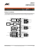
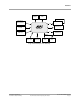
Features SATA Port Multiplier HDD PCI Express On Board DDR2 Mini Card Wi-Fi x16 SPI Flash (op.) SD Card 88F6281 x8 USB Host NAND Flash TDM Audio A/D – D/A GbE PHY FXS FXO Usage Model Example: VoIP Gateway Copyright © 2008 Marvell December 2, 2008, Preliminary Doc. No. MV-S104859-U0 Rev.
8F6281 Hardware Specifications Table of Contents Product Overview ....................................................................................................................................... 3 Features....................................................................................................................................................... 4 Preface.........................................................................................................................................
Table of Contents 8 Electrical Specifications (Preliminary) ...................................................................................... 75 8.1 Absolute Maximum Ratings ............................................................................................................................75 8.2 Recommended Operating Conditions .............................................................................................................77 8.3 Thermal Power Dissipation ...................
88F6281 Hardware Specifications List of Tables 1 Pin and Signal Descriptions ............................................................................................................ 17 Table 1: 2 Pin Functions and Assignments Table Key ......................................................................................19 Table 2: Interface Pin Prefix Codes ................................................................................................................
List of Tables 7 8 9 JTAG Interface .................................................................................................................................. 73 Table 33: Supported JTAG Instructions............................................................................................................73 Table 34: IDCODE Register Map .....................................................................................................................
88F6281 Hardware Specifications 10 Package ...........................................................................................................................................130 Table 73: 11 Part Order Numbering/Package Marking......................................................................................132 Table 74: A HSBGA 288-pin Package Dimensions ...........................................................................................131 88F6281 Part Order Options .............
List of Figures List of Figures 1 Pin and Signal Descriptions ........................................................................................................... 17 Figure 1: 88F6281 Pin Logic Diagram ............................................................................................................18 2 Unused Interface Strapping............................................................................................................ 49 3 88F6281 Pin Map and Pin List ..............
88F6281 Hardware Specifications 9 10 Figure 28: Inter-IC Sound (I2S) Test Circuit ....................................................................................................107 Figure 29: Inter-IC Sound (I2S) Output Delay AC Timing Diagram .................................................................108 Figure 30: Inter-IC Sound (I2S) Input AC Timing Diagram ..............................................................................108 Figure 31: TDM Interface Test Circuit .........
Preface About this Document Preface About this Document This datasheet provides the hardware specifications for the 88F6281 integrated controller. The hardware specifications include detailed pin information, configuration settings, electrical characteristics and physical specifications. This datasheet is intended to be the basic source of information for designers of new systems. In this document, the “88F6281” is often referred to as the “device”.
88F6281 Hardware Specifications RFC 1321 (The MD5 Message-Digest Algorithm) RFC 1851 – The ESP Triple DES Transform RFC 2104 (HMAC: Keyed-Hashing for Message Authentication). RFC 2405 – The ESP DES-CBC Cipher Algorithm With Explicit IV IEEE standard, 802.3-2000 Clause 14 ANSI standard X3.263-1995 See the Marvell Extranet website for the latest product documentation.
Pin and Signal Descriptions 1 Pin and Signal Descriptions This section provides the pin logic diagram for the 88F6281 device and a detailed description of the pin assignments and their functionality. Copyright © 2008 Marvell December 2, 2008, Preliminary Doc. No. MV-S104859-U0 Rev.
88F6281 Hardware Specifications 1.1 Pin Logic Figure 1: 88F6281 Pin Logic Diagram VDD VDD_CPU VDDO VDD_GE_A VDD_GE_B VDD_M VSS CPU_PLL_AVDD CPU_PLL_AVSS CORE_PLL_AVDD CORE_PLL_AVSS XTAL_AVDD XTAL_AVSS PEX_AVDD SATA0_AVDD SATA1_AVDD Misc.
Pin and Signal Descriptions Pin Descriptions 1.2 Pin Descriptions This section details all the pins for the different interfaces providing a functional description of each pin and pin attributes. Table 1 defines the abbreviations and acronyms used in the pin description tables.
88F6281 Hardware Specifications Table 2: Interface Pin Prefix Codes (Continued) In t e r f a c e P re fi x RTC RTC_ NAND Flash NF_ MPP N/A TWSI TW_ UART UA0_ UA1_ Audio AU_ SPI SPI_ SDIO SD_ TDM TDM_ PTP PTP_ Doc. No. MV-S104859-U0 Rev.
Pin and Signal Descriptions Pin Descriptions 1.2.1 Power Supply Pins Table 3 provides the voltage levels for the various interface pins. These do not include the analog power supplies for the PLLs or PHYs which are explicitly mentioned in the other pin description tables. Table 3: Power Pin Assignments Pin Name I /O Pi n Ty p e D es c r ip t i o n VDD I Power 1.0V Digital core voltage VDD_CPU I Power 1.1V Digital CPU voltage VDDO I Power 3.
88F6281 Hardware Specifications Table 3: Power Pin Assignments (Continued) Pin Name I /O Pi n Ty p e D es c r ip t i o n PEX_AVDD I Power PCI Express PHY quiet power supply 1.8V NOTE: See the 88F6180, 88F6190, 88F6192, and 88F6281 Design Guide for power supply filtering recommendations. SATA0_AVDD SATA1_AVDD I Power SATA II port0/1 quiet 3.3V power supply NOTE: See 88F6180, 88F6190, 88F6192, and 88F6281 Design Guide for power supply filtering recommendation. USB_AVDD I Power USB 2.
Pin and Signal Descriptions Pin Descriptions 1.2.2 Miscellaneous Pin Assignment The Miscellaneous signal list contains clock and reset, test, and related signals. Table 4: Miscellaneous Pin Assignments Pin Name I /O Pi n Ty pe P ow e r Rail D e s c r i p t io n REF_CLK_XIN I Analog XTAL_AVDD Reference clock input from external oscillator or input from external crystal. Used as input to core, CPU, SATA, and USB PLLs. XOUT O Analog XTAL_AVDD XTAL_OUT Feedback signal to external crystal.
88F6281 Hardware Specifications 1.2.3 Table 5: DDR SDRAM Interface Pin Assignments DDR SDRAM Interface Pin Assignments Pin Name I /O Pi n Ty pe P ow e r Rail D e s cr ip t i o n M_CLKOUT M_CLKOUTn O SSTL VDD_M SDRAM Differential Clock Pair M_CKE O SSTL VDD_M Driven high to enable SDRAM clock. Driven low when setting the SDRAM to Self-refresh mode. M_RASn O SSTL VDD_M SDRAM Row Address Select Asserted to indicate an active ROW address driven on the SDRAM address lines.
Pin and Signal Descriptions Pin Descriptions Table 5: DDR SDRAM Interface Pin Assignments (Continued) Pin Name I /O Pi n Ty pe P ow e r Rail D e s cr ip t i o n M_STARTBURST O SSTL VDD_M Start Burst 88F6281 indication of starting a burst read transaction. Asserted with the first M_CASn cycle of SDRAM access. NOTE: Must be routed on board to the SDRAM, and back to the 88F6281 as M_STARTBURST_IN.
88F6281 Hardware Specifications 1.2.4 Table 6: PCI Express Interface Pin Assignments PCI Express Interface Pin Assignments Pin Name I/O P in Ty p e Power R a il D e s c r i p t io n PEX_CLK_P/N I/O HCSL PEX_AVDD PCI Express Reference Clock 100 MHz, differential This clock can be configured as input or output according to the reset strap (see Table 32, Reset Configuration, on page 67). NOTE: For Output mode, 50-ohm, pull-down resistors are required.
Pin and Signal Descriptions Pin Descriptions 1.2.
88F6281 Hardware Specifications 1.2.6 Gigabit Ethernet Port Interface Pin Assignments For additional information about the Gigabit Ethernet port pin functions refer to Section 4.2, Gigabit Ethernet (GbE) Pins Multiplexing on MPP, on page 57. Table 8: Gigabit Ethernet Port0/1 Interface Pin Assignments Pin Name I/O P in Ty p e Power R a il D e s c r i p t io n VDD_GE_A RGMII Transmit Clock RGMII transmit reference output clock for GE_TXD[3:0] and GE_TXCTL. Provides 125 MHz, 25 MHz or 2.5 MHz clock.
Pin and Signal Descriptions Pin Descriptions Table 8: Gigabit Ethernet Port0/1 Interface Pin Assignments (Continued) Pin Name I/O P in Ty p e Power R a il D e s c r i p t io n GE_RXD[3:0] I CMOS VDD_GE_A RGMII Receive Data Contains the receive data nibble inputs that are synchronous to GE_RXCLK input rising/falling edge. MII/MMII Receive Data Contains the receive data nibble inputs that are synchronous to GE_RXCLK input. GMII Receive Data Contains the receive data nibble inputs.
88F6281 Hardware Specifications Table 8: Gigabit Ethernet Port0/1 Interface Pin Assignments (Continued) Pin Name I/O P in Ty p e Power R a il D e s c r i p t io n MPP[27:24]/ GE1[7:4] I CMOS VDD_GE_B RGMII Receive Data Contains the receive data nibble inputs that are synchronous to GE_RXCLK input rising/falling edge. MII/MMII Receive Data Contains the receive data nibble inputs that are synchronous to GE_RXCLK input. GMII Receive Data Contains the receive data nibble inputs.
Pin and Signal Descriptions Pin Descriptions Table 8: Gigabit Ethernet Port0/1 Interface Pin Assignments (Continued) Pin Name I/O P in Ty p e Power R a il D e s c r i p t io n MPP[32]/GE1[12] I/O CMOS VDD_GE_B RGMII Transmit Clock RGMII transmit reference output clock for GE_TXD[3:0] and GE_TXCTL Provides 125 MHz, 25 MHz or 2.5 MHz clock. Not used in MII/MMII mode. MII/MMII Carrier Sense Indicates that the receive medium is non-idle.
88F6281 Hardware Specifications 1.2.7 Table 9: Serial Management Interface (SMI) Interface Pin Assignments Serial Management Interface (SMI) Pin Assignments Pin Name I/O P in Ty p e Power R a il D e s c r i p t io n GE_MDC t/s O CMOS/ VDD_GE_A Management Data Clock MDC is derived from TCLK divided by 128. Provides the timing reference for the transfer of the MDIO signal.
Pin and Signal Descriptions Pin Descriptions 1.2.8 USB 2.0 Interface Pin Assignments Table 10: USB 2.0 Interface Pin Assignments Pin Name I/O Pi n Ty p e P ow e r R ai l D e s c r ip t i o n USB_DP USB_DM I/O CML USB_AVDD USB 2.0 Data Differential Pair Copyright © 2008 Marvell December 2, 2008, Preliminary Doc. No. MV-S104859-U0 Rev.
88F6281 Hardware Specifications 1.2.9 JTAG Interface Pin Assignment Table 11: JTAG Pin Assignment Pin Name I/O P in Ty p e Power R a il D e s c r i p t io n JT_CLK I CMOS VDDO JTAG Clock Clock input for the JTAG controller. NOTE: This pin is internally pulled down to 0. JT_RSTn I CMOS VDDO JTAG Reset When asserted, resets the JTAG controller. NOTE: This pin is internally pulled down to 0.1 JT_TMS_CPU I CMOS VDDO CPU JTAG Mode Select Controls CPU JTAG controller state.
Pin and Signal Descriptions Pin Descriptions 1.2.10 Real Time Clock (RTC) Interface Pin Assignments Table 12: RTC Interface Pin Assignments Pin Name I/O P in Ty p e Power R a il D e s c r i p t io n RTC_XIN I Analog RTC_AVDD RTC Crystal Clock Input RTC_XOUT O Analog RTC_AVDD RTC Crystal Clock Feedback Copyright © 2008 Marvell December 2, 2008, Preliminary Doc. No. MV-S104859-U0 Rev.
88F6281 Hardware Specifications 1.2.11 NAND Flash Interface Pin Assignment Table 13: NAND Flash Interface Pin Assignment Pin Name I/O P in Ty p e Power R a il D e s c r i p t io n NF_IO[7:0] I/O CMOS VDDO Data Input/Output Used to output command, address and data, and to input data during read operations.
Pin and Signal Descriptions Pin Descriptions 1.2.
88F6281 Hardware Specifications 1.2.13 Two-Wire Serial Interface (TWSI) Interface All of the TWSI signals are multiplexed on the MPP pins (see Section 4, Pin Multiplexing, Note on page 51). Table 15: Two-Wire Serial Interface (TWSI) Interface Pin Assignment Pin Name I/O P in Ty p e Power R a il D e s c r i p t io n TW_SDA o/d I/O CMOS VDDO TWSI Port Serial Data Address or write data driven by the TWSI master or read response data driven by the TWSI slave.
Pin and Signal Descriptions Pin Descriptions 1.2.14 UART Interface Note All of the UART signals are multiplexed on the MPP pins (see Section 4, Pin Multiplexing, on page 51).
88F6281 Hardware Specifications 1.2.15 Audio (S/PDIF / I2S) Interface Note All of the Audio signals are multiplexed on the MPP pins (see Section 4, Pin Multiplexing, on page 51). If the Audio interface is not used, leave all of the signals unconnected. The Audio signals are powered on VDDO or on VDD_GE_B, based on the pin multiplexing option.
Pin and Signal Descriptions Pin Descriptions 1.2.16 Serial Peripheral Interface (SPI) Interface All of the SPI signals are multiplexed on the MPP pins (see Section 4, Pin Multiplexing, Note on page 51). Table 18: Serial Peripheral Interface (SPI) Interface Signal Assignment I/O Pin Type Power Rail Description SPI_MOSI O CMOS VDDO SPI Data Output Data is output from the master and input to the slave. SPI_MISO2 I CMOS VDDO SPI Data Input Data is input to the master and output from the slave.
88F6281 Hardware Specifications 1.2.17 Secure Digital Input/Output (SDIO) Interface All of the SDIO signals are multiplexed on the MPP pins (see Section 4, Pin Multiplexing, Note on page 51). Table 19: Secure Digital Input/Output (SDIO) Interface Signal Assignment Pin Name I/O Pin Type Power Rail Description SD_CLK O CMOS VDDO SDIO Clock SD_CMD I/O CMOS VDDO SDIO Command Used to transfer a command serially from the SDIO host to the SDIO device.
Pin and Signal Descriptions Pin Descriptions 1.2.18 Time Division Multiplexing (TDM) Interface Note All of the TDM signals are multiplexed on the MPP pins (see Section 4, Pin Multiplexing, on page 51). The TDM signals are powered on VDDO or on VDD_GE_B, based on the pin multiplexing option (see Section 4, Pin Multiplexing, on page 51).
88F6281 Hardware Specifications Table 20: Time Division Multiplexing (TDM) Interface Signal Assignment (Continued) Pin Name I/O Pin Type Power Rail Description TDM_SPI_MOSI O CMOS VDDO/ VDD_GE_B Serial SPI data from the host to the codec for register access. When TDM_SPI_CS is asserted low, the data is driven from the host on the negative edge of TDM_SPI_SCK. It is always driven for eight TDM_SPI_SCK cycles at a time. In a byte, the data can be driven MSB or LSB first.
Pin and Signal Descriptions Pin Descriptions 1.2.19 Transport Stream (TS) Interface Note All of the TS signals are multiplexed on the MPP pins (see Section 4, Pin Multiplexing, on page 51). The TS signals are powered on VDDO or on VDD_GE_B based on the pin multiplexing option (see Section 4, Pin Multiplexing ).
88F6281 Hardware Specifications Table 21: Transport Stream (TS) Interface Signal Assignment (Continued) Pin Name I/O Pin Type Power Rail Description TSMP[7] I/O CMOS VDDO/ VDD_GE_B • • TSMP[8] I/O CMOS VDDO/ VDD_GE_B • • TSMP[9] I/O CMOS VDDO/ VDD_GE_B • • TSMP[10] I/O CMOS VDDO/ VDD_GE_B • • Parallel Mode: TS0_DATA[2]: Port0 TS Data bit 2 Serial Mode: TS1_SYNC: Port1 Sync/Frame Start Indicator or Packet Clock.
Pin and Signal Descriptions Pin Descriptions 1.2.20 Precise Timing Protocol (PTP) Interface Note All of the PTP signals are multiplexed on the MPP pins (see Section 4, Pin Multiplexing, on page 51). Table 22: Precise Timing Protocol (PTP) Interface Signal Assignment Pin Name I/O Pin Type Power Rail Description PTP_CLK I CMOS VDDO PTP Clock PTP_EVENT_REQ I CMOS VDDO Trigger generation to the PTP core. PTP_TRIG_GEN O CMOS VDDO Trigger generated by the PTP core.
88F6281 Hardware Specifications 1.3 Internal Pull-up and Pull-down Pins Some pins of the device package are connected to internal pull-up and pull-down resistors. When these pins are Not Connected (NC) on the system board, these resistors set the default value for input and sample at reset configuration pins. The internal pull-up and pull-down resistor value is 50 kΩ. An external resistor with a lower value can override this internal resistor.
Unused Interface Strapping 2 Unused Interface Strapping Table 24 lists the signal strapping to be used for systems in which some of the device interfaces are unused (not connected). Table 24: Unused Interface Strapping Unused Interface Str a pp i ng Ethernet SMI Pull up GE_MDIO. MPP Configure any unused MPP pin to GPIO output. Leave the power supply connected. • If the related power supply is VDDO, leave it connected to 3.3V.
88F6281 Hardware Specifications 3 88F6281 Pin Map and Pin List The 88F6281 pin list is provided as an Excel file attachment. To open the attached Excel pin list file, double-click the pin icons below: 88F6281 Pin Map and Pin List.xls File attachments are only supported by Adobe Reader 6.0 and above. Note To download the latest version of free Adobe Reader go to http://www.adobe.com. Doc. No. MV-S104859-U0 Rev.
Pin Multiplexing Multi-Purpose Pins Functional Summary 4 Pin Multiplexing 4.1 Multi-Purpose Pins Functional Summary The 88F6281 device contains 50 Multi-Purpose Pins (MPP). Each one can be assigned to a different functionality through the MPP Control register.
88F6281 Hardware Specifications MPP pins can be assigned to different functionalities through the MPP Control register, as shown in Table 25.
Pin Multiplexing Multi-Purpose Pins Functional Summary Table 26: MPP Function Summary Pin name 0x0 0x1 0x2 0x3 0x4 0x5 0xC 0xD MPP[0] GPIO[0] (in/out) NF_IO[2] (in/out) SPI_SCn (out) - - - - - MPP[1] GPO[1] (out only) NF_IO[3] (in/out) SPI_MOSI (out) - - - - - MPP[2] GPO[2] (out only) NF_IO[4] (in/out) SPI_SCK (out) - - - - - MPP[3] GPO[3] (out only) NF_IO[5] (in/out) SPI_MISO (in) - - - - - MPP[4] GPIO[4] (in/out) NF_IO[6] (in/out) UA0_RXD (in) - - SATA1_
88F6281 Hardware Specifications Table 26: MPP Function Summary (Continued) Pin name 0x0 0x1 0x2 0x3 0x4 0x5 0xC 0xD MPP[18] GPO[18] (out only) NF_IO[0] (in/out) - - - - - - MPP[19] GPO[19] (out only) NF_IO[1] (in/out) - - - - - - MPP[20] GPIO[20] (in/out) TSMP[0] (in/out) TDM_CH0_ TX_QL (out) GE1[0] AU_SPDIFI SATA1_AC (in) Tn (out) - - MPP[21] GPIO[21] (in/out) TSMP[1] (in/out) TDM_CH0_ RX_QL (out) GE1[1] AU_SPDIF SATA0_AC O (out) Tn (out) - - MPP[22] GPIO[22] (i
Pin Multiplexing Multi-Purpose Pins Functional Summary Table 26: MPP Function Summary (Continued) Pin name 0x0 0x1 0x2 0x3 0x4 0x5 0xC 0xD MPP[36] GPIO[36] (in/out) TSMP[0] (in/out) TDM_SPI_ CS1 (out) - AU_SPDIFI (in) - - - MPP[37] GPIO[37] (in/out) TSMP[1] (in/out) TDM_CH2_ TX_QL (out) - AU_SPDIF O (out) - - - MPP[38] GPIO[38] (in/out) TSMP[2] (in/out) TDM_CH2_ RX_QL (out) - AU_SPDIF RMCLK (out) - - - MPP[39] GPIO[39] (in/out) TSMP[3] (in/out) TDM_SPI_ CS0 (out) -
88F6281 Hardware Specifications Note For MPPs assigned as NAND flash and SPI flash, wake-up mode after reset depends on Boot mode (see the Boot Device field in Table 32, Reset Configuration, on page 67): • When Boot mode is NAND Flash, MPP[5:0] and MPP[19:18] wake up after reset in NAND Flash mode. • When Boot mode is SPI Flash, either MPP[3:0] or {MPP[3:1] and MPP[7]} wake up after reset in SPI mode, (according to boot mode configured by reset strap pins).
Pin Multiplexing Gigabit Ethernet (GbE) Pins Multiplexing on MPP 4.2 Gigabit Ethernet (GbE) Pins Multiplexing on MPP The 88F6281 has 14 dedicated pins for its GbE port. (12 RGMII pins, an MDC pin, and an MDIO pin). For the 88F6281, additional GbE interface pins are multiplexed on the MPPs, to serve as the following interfaces to an external PHY or switch.
88F6281 Hardware Specifications Table 27: Ethernet Ports Pins Multiplexing (Continued) Pin Name 1x GMII RGMII0 +MII1/ MM I I1 2x RGMII MII0/MMII0+ R GM I I1 MPP_34 / GE1[14] NA MII1_TXEN (out) NA NA MPP_35 / GE1[15] NA MII1_RXERR (in) NA NA Note When using Gigabit Ethernet signals on MPPs, all relevant Gigabit Ethernet signals (except those marked as NA) must be implemented.
Pin Multiplexing TSMP (TS Multiplexing Pins) on MPP 4.3 TSMP (TS Multiplexing Pins) on MPP The TS interface can be configured to one of five modes: One or two serial in interfaces One or two serial out interfaces Serial in and serial out interface Parallel in interface Parallel out interface In parallel in or serial in mode, all TS signals are inputs. In parallel out or serial out mode, all TS signals are outputs. Table 28 summarizes the TS port pins multiplexing.
88F6281 Hardware Specifications 5 Clocking Table 29 lists the clocks in the 88F6281. Table 29: 88F6281Clocks C l o ck Ty p e Description CPU PLL • Reference clock: REF_CLK_XIN (25 MHz) • Derivative clocks: - CPU clock - L2 cache clock - DDR Clock (the Mbus-L uses the DDR clock.) NOTE: See Table 32, Reset Configuration, on page 67 for CPU, L2 cache and DDR frequency configuration. L2 cache clock frequency must be equal or higher then DDR clock frequency.
Clocking Table 29: 88F6281Clocks (Continued) C l o ck Ty p e Description SATA PHY PLL • • Reference clock: REF_CLK_XIN (25 MHz) Derivative clock: SATA Clock (150 MHz) RTC • Reference clock: RTC_XIN (32.768 kHz) Used for real time clock functionality, see the Real Time Clock section in the 88F6180, 88F6190, 88F6192, and 88F6281 Functional Specifications.
88F6281 Hardware Specifications 5.1 Spread Spectrum Clock Generator (SSCG) The SSCG (Spread Spectrum Clock Generator) may be used to generate the spread spectrum clock for the PLL input. See SSCG Disable in Table 32, Reset Configuration, on page 67, for SSCG enable/bypass configuration settings. The SSCG block can be configured to perform up spread, down spread and center spread. The modulation frequency is configurable. Typical frequency is 30 kHz. The spread percentage can also be configured up to 1%.
System Power Up/Down and Reset Settings Power-Up/Down Sequence Requirements 6 System Power Up/Down and Reset Settings This section provides information about the device power-up/down sequence and configuration at reset. 6.1 Power-Up/Down Sequence Requirements 6.1.
88F6281 Hardware Specifications Figure 2: Power-Up Sequence Example Voltage Non-Core Voltage 70% of Non-Core Voltage Core Voltage 70% of Core Voltage Reset(s) Clock(s) Note 6.1.2 It is the designer's responsibility to verify that the power sequencing requirements of other components are also met.
System Power Up/Down and Reset Settings Hardware Reset Note 6.2.1 Reset (SYSRSTn signal) must be active for a minimum length of 5 ms. core power, I/O power, and analog power must be stable (VDD +/- 5%) during that time and onward. Reset Out Signal The device has an optional SYSRST_OUTn output signal, multiplexed on an MPP pin, that is used as a reset request from the device to the board reset logic. SYSRST_OUTn is the default option for that MPP pin.
88F6281 Hardware Specifications 6.3 PCI Express Reset 6.3.1 PCI Express Root Complex Reset As a Root Complex, the device may generate a Hot Reset to the PCI Express port. Upon CPU setting the PCI Express Control register’s bit, the PCI Express unit sends a Hot Reset indication to the Endpoint, see the PCI Express Interface section in the 88F6180, 88F6190, 88F6192, and 88F6281 Functional Specifications. 6.3.
System Power Up/Down and Reset Settings Pins Sample Configuration Note If external logic is used instead of pull-up and pull-down resistors, the logic must drive all of these signals to the desired values during SYSRSTn assertion. To prevent bus contention on these pins, the external logic must float the bus no later than the third TCLK cycle after SYSRSTn de-assertion.
88F6281 Hardware Specifications Table 32: Reset Configuration (Continued) P in C on fi g ur a tio n F u n ct io n MPP[33], NF_ALE, NF_REn, NF_CLE CPU_CLK to DDR CLK Ratio 0x0–0x3 = Reserved 0x4 = 3:1 0x5 = Reserved 0x6 = 4:1 0x7 = 4.5:1 0x8 = 5:1 0x9 = 6:1 0xA–0xF = Reserved NOTE: Internally pulled to 0x4. The supported combination for CPU_CLK Frequency select, CPU_CLK to DDR CLK ratio, and CPU_CLK to CPU L2 clock ratio are listed in Table 30, Supported Clock Combinations, on page 61.
System Power Up/Down and Reset Settings Pins Sample Configuration Table 32: Reset Configuration (Continued) P in C on fi g ur a tio n F u n ct io n GE_TXD[2:0] Boot Device 0x0 = Reserved 0x1 = Reserved 0x2 = Boot from SPI flash (SPI_CSn on MPP[7]) 0x3 = Reserved 0x4 = Boot from SPI flash (SPI_CSn on MPP[0]) 0x5 = Boot from NAND flash 0x6 = Boot from SATA 0x7 = Boot from the PCI Express port NOTE: • Internally pulled to 0x4.
88F6281 Hardware Specifications Table 32: Reset Configuration (Continued) P in C on fi g ur a tio n F u n ct io n MPP[18] Reserved NOTE: MUST be externally pulled down to 0x0 during reset. 6.6 Serial ROM Initialization The device supports initialization of ALL of its internal and configuration registers through the TWSI master interface.
System Power Up/Down and Reset Settings Boot Sequence The serial ROM initialization logic reads eight bytes at a time. It performs address decoding on the 32-bit address being read, and based on address decoding result, writes the next four bytes to the required target. The Serial Initialization Last Data Register contains the expected value of last serial data item (default value is 0xFFFFFFFF). When the device reaches last data, it stops the initialization sequence. 6.6.
88F6281 Hardware Specifications Upon completing the above sequence, the internal CPU reset is de-asserted, and the CPU starts executing boot code from the boot device (SPI flash, NAND flash, or internal Boot ROM), according to sample at reset setting, see Table 32, Reset Configuration, on page 67. For bootROM details, see the BootROM section in the 88F6180, 88F6190, 88F6192, and 88F6281 Functional Specifications.
JTAG Interface TAP Controller 7 JTAG Interface To enable board testing, the device supports a test mode operation through its JTAG boundary scan interface. The JTAG interface is IEEE 1149.1 standard compliant. It supports mandatory and optional boundary scan instructions. 7.1 TAP Controller The Test Access Port (TAP) is constructed with a 5-pin interface and a 16-state Finite State Machine (FSM), as defined by IEEE JTAG standard 1149.1.
88F6281 Hardware Specifications 7.3 Bypass Register The Bypass register (BR) is a single bit serial shift register that connects TDI to TDO, when the IR holds the Bypass command, and the TAP FSM is in Shift-DR state. Data that is driven on the TDI input pin is shifted out one cycle later on the TDO output pin. The Bypass register is loaded with 0 when the TAP FSM is in the Capture-DR state. 7.
Electrical Specifications (Preliminary) Absolute Maximum Ratings 8 Electrical Specifications (Preliminary) The numbers specified in this section are PRELIMINARY and SUBJECT TO CHANGE. Note 8.1 Absolute Maximum Ratings Table 35: Absolute Maximum Ratings Parameter Min Max U n its C om m e n ts VDD -0.5 1.2 V Core voltage VDD_CPU -0.5 1.32 V CPU interface CPU_PLL_AVDD CORE_PLL_AVDD -0.5 2.2 V Analog supply for the internal PLL SSCG_AVDD -0.5 2.
88F6281 Hardware Specifications Table 35: Absolute Maximum Ratings (Continued) Parameter Min Max U n its C om m e n ts RTC_AVDD -0.5 2.2 V Analog supply for: RTC interface TC -40 125 °C Case temperature TSTG -40 125 °C Storage temperature Caution Exposure to conditions at or beyond the maximum rating may damage the device. Operation beyond the recommended operating conditions (Table 36) is neither recommended nor guaranteed. Doc. No. MV-S104859-U0 Rev.
Electrical Specifications (Preliminary) Recommended Operating Conditions 8.2 Recommended Operating Conditions Table 36: Recommended Operating Conditions Parameter M in Ty p Max Units C om m e n ts VDD 0.95 1.0 1.05 V Core voltage VDD_CPU 1.05 1.1 1.15 V CPU interface CPU_PLL_AVDD CORE_PLL_AVDD 1.7 1.8 1.9 V Analog supply for the internal PLL SSCG_AVDD 1.7 1.8 1.9 V Analog supply for: Internal Spread Spectrum Clock Generator VDD_GE_A VDD_GE_B 3.15 3.3 3.
88F6281 Hardware Specifications Table 36: Recommended Operating Conditions (Continued) Parameter M in Ty p Max Units C om m e n ts XTAL_AVDD 1.7 1.8 1.9 V Analog supply for: Internal clock inverter for crystal support and current source for SATA and USB PHYs RTC_AVDD 1.7 1.8 1.9 V Analog supply for RTC in Regular mode 1.3 1.5 1.
Electrical Specifications (Preliminary) Thermal Power Dissipation 8.3 Thermal Power Dissipation Note Before designing a system, Marvell recommends reading application note AN-63: Thermal Management for Marvell Technology Products. This application note presents basic concepts of thermal management for integrated circuits (ICs) and includes guidelines to ensure optimal operating conditions for Marvell Technology's products.
88F6281 Hardware Specifications 8.4 Current Consumption The purpose of the Current Consumption table is to support board power design and power module selection. . Table 38: Current Consumption In t e r f a c e S y m bo l Te s t C on d it io n s Max Units Core (VDD 1.0V) IVDD TCLK @ 200 MHz 600 mA Embedded CPU (VDD_CPU 1.1V) IVDD_CPU CPU @ 1000 MHz, L2 @ 333 MHz 1920 mA CPU @ 1200 MHz, L2 @ 400 MHz 2010 mA CPU @ 1500 MHz, L2 @ 500 MHz 2100 mA RGMII 1.8V or 3.
Electrical Specifications DC Electrical Specifications 8.5 DC Electrical Specifications Note 8.5.1 See Section 1.3, Internal Pull-up and Pull-down Pins, on page 48 for internal pullup/pulldown information. General 3.
88F6281 Hardware Specifications 8.5.2 RGMII, SMI and REF_CLK_XIN 1.8V (CMOS) DC Electrical Specifications In the following table, for the RGMII interface, VDDIO means the VDD_GE_A power rail. In the following table, for the REF_CLK_XIN pin, VDDIO means the XTAL_AVDD power rail. Table 40: RGMII 1.8V Interface (CMOS) DC Electrical Specifications Param eter Sym bol Test Condition Min Typ Max Units Notes Input low level VIL -0.3 0.35*VDDIO V - Input high level VIH 0.65*VDDIO VDDIO+0.
Electrical Specifications DC Electrical Specifications 8.5.3 SDRAM DDR2 Interface DC Electrical Specifications In the following table, VREF is VDD_M/2 and VDDIO means the VDD_M power rail. Table 41: SDRAM DDR2 Interface DC Electrical Specifications Parameter Input low level Symbol Test Condition Min Typ Max Units Notes VIL - -0.3 VREF - 0.125 V - Input high level VIH - VREF + 0.125 VDDIO + 0.3 V - Output low level VOL IOL = 13.4 mA 0.28 V - Output high level VOH IOH = -13.
88F6281 Hardware Specifications 8.5.4 Two-Wire Serial Interface (TWSI) 3.3V DC Electrical Specifications In the following table, VDDIO means the VDDO power rail. Table 42: TWSI Interface 3.3V DC Electrical Specifications Param eter Sym bol Test Condition Min Typ Max Units Notes Input low level VIL -0.5 0.3*VDDIO V - Input high level VIH 0.7*VDDIO VDDIO+0.5 V - Output low level VOL IOL = 3 mA - 0.
Electrical Specifications DC Electrical Specifications 8.5.6 Time Division Multiplexing (TDM) 3.3V DC Electrical Specifications In the following table VDDIO means the either the VDDO or the VDD_GE_B power rail, depending on which MPP pins are configured for the TDM interface. Table 44: TDM Interface 3.3V DC Electrical Specifications Param eter Sym bol Test Condition Min Typ Max Units Notes Input low level VIL -0.5 0.3*VDDIO V - Input high level VIH 0.7*VDDIO VDDIO+0.
88F6281 Hardware Specifications 8.6 AC Electrical Specifications See Section 8.7, Differential Interface Electrical Characteristics, on page 118 for differential interface specifications. 8.6.1 Reference Clock AC Timing Specifications Table 45: Reference Clock AC Timing Specifications D e s c r i p t io n Sy m b o l Min Max Units Frequency FREF_CLK_XIN 25 50 ppm 25 + 50 ppm MHz Clock duty cycle DCREF_CLK_XIN 40 60 % Slew rate SRREF_CLK_XIN 0.
Electrical Specifications AC Electrical Specifications Table 45: Reference Clock AC Timing Specifications (Continued) D e s c r i p t io n Sy m b o l Min Max Units Notes T D M _ S PI O u tp ut C lo c k TDM_SPI output clock 8.
F6281 Hardware Specifications 8.6.2 SDRAM DDR2 Interface AC Timing 8.6.2.1 SDRAM DDR2 Interface AC Timing Table Table 46: SDRAM DDR2 Interface AC Timing Table 400 MHz @ 1.8V Description Min Sym bol Clock frequency fCK Max 400.0 - Notes MHz - ns - DQ and DM valid output time before DQS transition tDOVB DQ and DM valid output time after DQS transition tDOVA 0.40 - ns - DQ and DM output pulse w idth tDIPW 0.35 - tCK(avg) - DQS output high pulse w idth tDQSH 0.
Electrical Specifications AC Electrical Specifications Table 47: SDRAM DDR2 Interface Address Timing Table 400 MHz @ 1.8V Sym bol Min Max Units Notes Address and Control valid output time before CLK-CLkn rising edge Description tAOVB 0.65 - ns 1, 2 Address and Control valid output time after CLK-CLKn rising edge tAOVA 0.65 - ns 1, 2 Address and Control valid output time before CLK-CLkn rising edge tAOVB 2.
88F6281 Hardware Specifications 8.6.2.
Electrical Specifications AC Electrical Specifications 8.6.2.3 SDRAM DDR2 Interface Test Circuit Figure 5: SDRAM DDR2 Interface Test Circuit VTT Test Point 50 ohm CL 8.6.2.4 SDRAM DDR2 Interface AC Timing Diagrams Figure 6: SDRAM DDR2 Interface Write AC Timing Diagram CLK tCH tDSH tDSS tDQSH tDQSL tCL CLKn DQS tWPRE tWPST DQSn tDIPW DQ tDOVB tDOVA Copyright © 2008 Marvell December 2, 2008, Preliminary Doc. No. MV-S104859-U0 Rev.
88F6281 Hardware Specifications Figure 7: SDRAM DDR2 Interface Address and Control AC Timing Diagram CLK tCH tCL CLKn tIPW ADDRESS/ CONTROL tAOVB tAOVA Figure 8: SDRAM DDR2 Interface Read AC Timing Diagram DQS DQSn DQ tDSI tDHI Doc. No. MV-S104859-U0 Rev.
Electrical Specifications AC Electrical Specifications 8.6.3 Reduced Gigabit Media Independent Interface (RGMII) AC Timing 8.6.3.1 RGMII AC Timing Table Table 49: RGMII 10/100/1000 AC Timing Table at 1.8V Description Sym bol Clock frequency fCK Data to Clock output skew Data to Clock input skew Min Max 125.0 Units Notes MHz - Tskew T -0.50 0.50 ns 2 Tskew R 1.00 2.60 ns - Clock cycle duration Tcyc 7.20 8.80 ns 1,2 Duty cycle for Gigabit Duty_G 0.45 0.
88F6281 Hardware Specifications 8.6.3.2 RGMII Test Circuit Figure 9: RGMII Test Circuit Test Point CL 8.6.3.3 RGMII AC Timing Diagram Figure 10: RGMII AC Timing Diagram TX CLOCK (At Transmitter) TX DATA TskewT RX CLOCK (At Receiver) RX DATA TskewR Doc. No. MV-S104859-U0 Rev.
Electrical Specifications AC Electrical Specifications 8.6.4 Gigabit Media Independent Interface (GMII) AC Timing 8.6.4.1 GMII AC Timing Table Table 51: GMII AC Timing Table 125 MHz Description GTX_CLK cycle time Sym bol Min Max Units Notes tCK 7.5 8.5 ns - RX_CLK cycle time tCKrx 7.5 - ns - GTX_CLK and RX_CLK high level w idth tHIGH 2.5 - ns 1 GTX_CLK and RX_CLK low level w idth tLOW 2.5 - ns 1 tR - 1.
88F6281 Hardware Specifications 8.6.4.3 GMII AC Timing Diagrams Figure 12: GMII Output AC Timing Diagram tLOW tHIGH VIH(min) GTX_CLK VIL(max) VIH(min) TXD, TX_EN, TX_ER VIL(max) tOVB tOVA Figure 13: GMII Input AC Timing Diagram tLOW tHIGH VIH(min) RX_CLK VIL(max) VIH(min) RXD, RX_EN, RX_ER VIL(max) tSETUP tHOLD Doc. No. MV-S104859-U0 Rev.
Electrical Specifications AC Electrical Specifications 8.6.5 Media Independent Interface/Marvell Media Independent Interface (MII/MMII) AC Timing 8.6.5.1 MII/MMII MAC Mode AC Timing Table Table 52: MII/MMII MAC Mode AC Timing Table Sym bol Min Max Units Notes Data input setup relative to RX_CLK rising edge Description tSU 3.5 - ns - Data input hold relative to RX_CLK rising edge tHD 2.0 - ns - Data output delay relative to MII_TX_CLK rising edge tOV 0.0 10.
88F6281 Hardware Specifications Figure 16: MII/MMII MAC Mode Input AC Timing Diagram Vih(min) RX_CLK Vih(min) RXD, RX_EN, RX_ER Vil(max) tSU tHD Doc. No. MV-S104859-U0 Rev.
Electrical Specifications AC Electrical Specifications 8.6.6 Serial Management Interface (SMI) AC Timing 8.6.6.1 SMI Master Mode AC Timing Table Table 53: SMI Master Mode AC Timing Table Description Sym bol Min Max See note 2 Units Notes MHz 2 MDC clock frequency fCK MDC clock duty cycle tDC 0.4 0.6 tCK - MDIO input setup time relative to MDC rise time tSU 40.0 - ns - MDIO input hold time relative to MDC rise time tHO 0.
88F6281 Hardware Specifications Figure 18: MDC Master Mode Test Circuit Test Point MDC CL 8.6.6.3 SMI Master Mode AC Timing Diagrams Figure 19: SMI Master Mode Output AC Timing Diagram VIH(min) MDC VIH(min) MDIO VIL(max) tOVB tOVA Figure 20: SMI Master Mode Input AC Timing Diagram VIH(min) MDC VIH(min) MDIO VIL(max) tSU tHO Doc. No. MV-S104859-U0 Rev.
Electrical Specifications AC Electrical Specifications 8.6.7 JTAG Interface AC Timing 8.6.7.1 JTAG Interface AC Timing Table Table 54: JTAG Interface AC Timing Table 30 MHz Description Sym bol Min Max 30.0 Units Notes JTClk frequency fCK MHz - JTClk minimum pulse w idth Tpw 0.45 0.55 tCK - JTClk rise/fall slew rate Sr/Sf 0.50 - V/ns 2 JTRSTn active time Trst 1.0 - ms - TMS, TDI input setup relative to JTClk rising edge Tsetup 6.
88F6281 Hardware Specifications 8.6.7.3 JTAG Interface AC Timing Diagrams Figure 22: JTAG Interface Output Delay AC Timing Diagram Tprop (max) JTCK VIH VIL TDO Tprop (min) Figure 23: JTAG Interface Input AC Timing Diagram JTCK TMS,TDI Tsetup Thold Doc. No. MV-S104859-U0 Rev.
Electrical Specifications AC Electrical Specifications 8.6.8 Two-Wire Serial Interface (TWSI) AC Timing 8.6.8.1 TWSI AC Timing Table Table 55: TWSI Master AC Timing Table Description Sym bol SCK clock frequency fCK Min Max See note 1 Units Notes kHz 1 SCK minimum low level w idth tLOW 0.47 - tCK 2 SCK minimum high level w idth tHIGH 0.40 - tCK 2 SDA input setup time relative to SCK rising edge tSU 250.0 - ns - SDA input hold time relative to SCK falling edge tHD 0.
88F6281 Hardware Specifications 8.6.8.2 TWSI Test Circuit Figure 24: TWSI Test Circuit VDDIO Test Point RL CL 8.6.8.3 TWSI AC Timing Diagrams Figure 25: TWSI Output Delay AC Timing Diagram tHIGH tLOW Vih(min) SCK Vil(max) Vih(min) SDA Vil(max) tOV(min) tOV(max) Figure 26: TWSI Input AC Timing Diagram tLOW tHIGH Vih(min) SCK Vil(max) Vih(min) SDA Vil(max) tSU tHD Doc. No. MV-S104859-U0 Rev.
Electrical Specifications AC Electrical Specifications 8.6.9 Sony/Philips Digital Interconnect Format (S/PDIF) AC Timing 8.6.9.1 S/PDIF AC Timing Table Table 57: S/PDIF AC Timing Table Description Sym bol Min Max Units Notes Output frequency accuracy Ftxtol -50.0 50.0 ppm 1 Input frequency accuracy Frxtol -100.0 100.0 ppm - Txjit - 0.05 UI 1, 2 Txjitgain - 3.0 dB 3 - 10.0 UI 4 - 0.25 UI 5 - 0.
88F6281 Hardware Specifications 8.6.9.2 S/PDIF Test Circuit Figure 27: S/PDIF Test Circuit Test Point CL Doc. No. MV-S104859-U0 Rev.
Electrical Specifications AC Electrical Specifications 8.6.10 Inter-IC Sound Interface (I2S) AC Timing 8.6.10.1 Inter-IC Sound (I2S) AC Timing Table Table 58: Inter-IC Sound (I2S) AC Timing Table Description Sym bol I2SBCLK clock frequency I2SBCLK clock high/low level pulse w idth Min Max See note 2 fCK Units Notes MHz 2 tCH/tCL 0.37 - tCK 1 I2SDI input setup time relative to I2SBCLK rise time tSU 0.10 - tCK - I2SDI input hold time relative to I2SBCLK rise time tHO 0.
88F6281 Hardware Specifications 8.6.10.3 Inter-IC Sound (I2S) AC Timing Diagrams Figure 29: Inter-IC Sound (I2S) Output Delay AC Timing Diagram tCL tCH VIH(min) I2SBCLK VIL(max) VIH(min) I2SDO, I2SLRCLK VIL(max) tODmin tODmax Figure 30: Inter-IC Sound (I2S) Input AC Timing Diagram tCL tCH VIH(min) I2SBCLK VIL(max) VIH(min) I2SDI VIL(max) tSU tHO Doc. No. MV-S104859-U0 Rev.
Electrical Specifications AC Electrical Specifications 8.6.11 Time Division Multiplexing (TDM) Interface AC Timing 8.6.11.1 TDM Interface AC Timing Table Table 59: TDM Interface AC Timing Table 8.192 MHz Description Sym bol Min Max Units Notes PCLK cycle time 1/tC 0.256 8.192 MHz 1, 3 PCLK duty cycle tDTY 0.4 0.6 tC 1 PCLK rise/fall time tR/tF - 3.0 ns 1, 2, 8 tD 0.0 20.0 ns 1, 4, 6 DRX and FSYNC setup time relative to PCLK falling edge tSU 10.
88F6281 Hardware Specifications 8.6.11.3 TDM Interface Timing Diagrams Figure 32: TDM Interface Output Delay AC Timing Diagram tC PCLK DTX tD tD Figure 33: TDM Interface Input Delay AC Timing Diagram tC PCLK DRX tSU tHD Doc. No. MV-S104859-U0 Rev.
Electrical Specifications AC Electrical Specifications 8.6.12 Serial Peripheral Interface (SPI) AC Timing 8.6.12.1 SPI (Master Mode) AC Timing Table Table 60: SPI (Master Mode) AC Timing Table SPI Description Sym bol Min Max See Note 3 Units Notes MHz 3 tCK 1 SCLK clock frequency fCK SCLK high time tCH 0.46 SCLK low time tCL 0.46 - tCK 1 SCLK slew rate tSR 0.5 - V/ns 1 Data out valid relative to SCLK falling edge tDOV -2.5 2.
88F6281 Hardware Specifications 8.6.12.3 SPI (Master Mode) Timing Diagrams Figure 35: SPI (Master Mode) Output AC Timing Diagram tCH tCL SCLK Data Out tDOVmin tDOVmax CS tCSB tCSA Figure 36: SPI (Master Mode) Input AC Timing Diagram SCLK Data in tSU tHD Doc. No. MV-S104859-U0 Rev.
Electrical Specifications AC Electrical Specifications 8.6.13 Secure Digital Input/Output (SDIO) Interface AC Timing 8.6.13.1 Secure Digital Input/Output (SDIO) AC Timing Table Table 61: SDIO Host in High Speed Mode AC Timing Table Description Symbol Min Max Units Notes fCK 0 50 MHz - Clock high/low level pulse w idth tWL/tWH 0.35 - tCK 1, 3 Clock rise/fall time tTLH/tTHL - 3.0 ns 1, 3 CMD, DAT output valid before CLK rising edge tDOVB 6.
88F6281 Hardware Specifications 8.6.13.3 Secure Digital Input/Output (SDIO) AC Timing Diagrams Figure 38: SDIO Host in High Speed Mode Output AC Timing Diagram tWL tWH VIH(min) VDDIO/2 CLK VIL(max) VIH(min) DAT, CMD VIL(max) tDOVB tDOVA Figure 39: SDIO Host in High Speed Mode Input AC Timing Diagram tWL tWH VIH(min) VDDIO/2 CLK VIL(max) VIH(min) DAT, CMD VIL(max) tISU tIHD Doc. No. MV-S104859-U0 Rev.
Electrical Specifications AC Electrical Specifications 8.6.14 Transport Stream (TS) Interface AC Timing 8.6.14.1 Transport Stream Interface AC Timing Table Table 62: Transport Stream Output Interface AC Timing Table Description Sym bol Clock frequency Min Max See note 1 fCK Units Notes MHz 1 Clock minimum low level w idth tLOW 0.4 0.6 tCK 2 Clock minimum high level w idth tHIGH 0.4 0.6 tCK 2 tOV 0.4 0.
88F6281 Hardware Specifications 8.6.14.2 Transport Stream Interface Test Circuit Figure 40: Transport Stream Interface Test Circuit Test Point CL 8.6.14.3 Transport Stream Interface Timing Diagrams Figure 41: Transport Stream Output Interface AC Timing Diagram tHIGH tLOW Vih(min) Clock Vil(max) Vih(min) Data Out Vil(max) tOV(min) tOV(max) Doc. No. MV-S104859-U0 Rev.
Electrical Specifications AC Electrical Specifications Figure 42: Transport Stream Input Interface AC Timing Diagram tLOW tHIGH Vih(min) Clock Vil(max) Vih(min) Data In Vil(max) tSU tHD Copyright © 2008 Marvell December 2, 2008, Preliminary Doc. No. MV-S104859-U0 Rev.
88F6281 Hardware Specifications 8.7 Differential Interface Electrical Characteristics This section provides the reference clock, AC, and DC characteristics for the following differential interfaces: PCI Express Interface Electrical Characteristics SATA Interface Electrical Characteristics USB Electrical Characteristics 8.7.1 Differential Interface Reference Clock Characteristics 8.7.1.
Electrical Specifications Differential Interface Electrical Characteristics PCI Express Interface Spread Spectrum Requirements Table 65: PCI Express Interface Spread Spectrum Requirements Min Max Units Notes Fmod Sym bol 0.0 33.0 kHz 1 Fspread -0.5 0.0 % 1 Notes: 1. Defined on linear sw eep or “Hershey’s Kiss” (US Patent 5,631,920) modulations. Copyright © 2008 Marvell December 2, 2008, Preliminary Doc. No. MV-S104859-U0 Rev.
88F6281 Hardware Specifications 8.7.2 PCI Express Interface Electrical Characteristics 8.7.2.1 PCI Express Interface Driver and Receiver Characteristics Table 66: PCI Express Interface Driver and Receiver Characteristics Units Notes Baud rate Description Sym bol BR 2.5 Gbps - Unit interval UI 400.0 ps - Baud rate tolerance Bppm Min Max -300.0 300.0 ppm 2 Driver parameters Differential peak to peak output voltage VTXpp 0.8 1.2 V - Minimum TX eye w idth TTXeye 0.
Electrical Specifications Differential Interface Electrical Characteristics 8.7.2.2 PCI Express Interface Test Circuit Figure 43: PCI Express Interface Test Circuit Test Points + C_TX D+ D- C_TX 50 ohm 50 ohm When measuring Transmitter output parameters, C_TX is an optional portion of the Test/Measurement load. When used, the value of C_TX must be in the range of 75 nF to 200 nF. C_TX must not be used when the Test/Measurement load is placed in the Receiver package reference plane.
88F6281 Hardware Specifications 8.7.3 SATA Interface Electrical Characteristics The driver and receiver characteristics for the SATA-I Interface Gen1i Mode and the SATA-II Interface Gen2i Mode are provided in the following sections. Doc. No. MV-S104859-U0 Rev.
Electrical Specifications Differential Interface Electrical Characteristics 8.7.3.1 SATA-I Interface Gen1i Mode Driver and Receiver Characteristics Table 67: SATA-I Interface Gen1i Mode Driver and Receiver Characteristics Description Sym bol Baud Rate Min Max 1.5 BR Units Notes Gbps - Baud rate tolerance Bppm -350.0 350.0 ppm Spread spectrum modulation frequency Fssc 30.0 33.0 kHz - Spread spectrum modulation Deviation SSCtol -5000.0 0.0 ppm - ps - Unit Interval 666.
88F6281 Hardware Specifications 8.7.3.2 SATA-II Interface Gen2i Mode Driver and Receiver Characteristics Table 68: SATA-II Interface Gen2i Mode Driver and Receiver Characteristics Description Baud Rate Baud rate tolerance Sym bol Min Max BR Bppm 3.0 -350.0 350.0 Units Notes Gbps - ppm - Spread spectrum modulation frequency Fssc 30.0 33.0 kHz - Spread spectrum modulation Deviation SSCtol -5000.0 0.0 ppm - ps 1,2 Unit Interval UI 333.
Electrical Specifications Differential Interface Electrical Characteristics 8.7.4 USB Electrical Characteristics 8.7.4.
88F6281 Hardware Specifications Table 70: USB Full Speed Driver and Receiver Characteristics Full Speed Description Sym bol BR Bppm Driver Parameters Ouput single ended high VOH Ouput single ended low VOL Output signal crossover voltage VCRS Output rise time TFR Output fall time TFL Source jitter total: to next transition TDJ1 Source jitter total: for paired transitions TDJ2 Source jitter for differential transition to SE0 transition TFDEOP Receiver Parameters Input single ended high VIH Input single ende
Electrical Specifications Differential Interface Electrical Characteristics Table 71: USB High Speed Driver and Receiver Characteristics High Speed Description Baud Rate Baud rate tolerance Data signaling high Data signaling low Data rise time Data fall time Data source jitter Sym bol BR Bppm Driver Parameters VHSOH VHSOL THSR THSF Min Max 480.0 -500.0 500.0 Units Mbps ppm Notes - 360.0 440.0 -10.0 10.0 500.0 500.
88F6281 Hardware Specifications Figure 45: High Speed TX Eye Diagram Pattern Template +525mV +475mV +400mV Differential +300mV 0 Volts Differential -300mV - 400mV Differential -475mV -525mV 7.5% 37.5% 92.5% 62.5% 0% 100% Figure 46: High Speed RX Eye Diagram Pattern Template +525mV +475mV +400mV Differential +175mV 0 Volts Differential -175mV - 400mV Differential -475mV -525mV 12.5% 35 65 0% Doc. No. MV-S104859-U0 Rev. E Page 128 87.
Thermal Data (Preliminary) 9 Thermal Data (Preliminary) Table 72 provides the package thermal data for the device. This data is derived from simulations that were run according to the JEDEC standard. The thermal parameters are preliminary and subject to change. Note TET The documents listed below provide a basic understanding of thermal management of integrated circuits (ICs) and guidelines to ensure optimal operating conditions for Marvell products.
88F6281 Hardware Specifications 10 Package This section provides the 88F6281 package drawing and dimensions. Figure 47: HSBGA 288-pin Package and Dimensions Doc. No. MV-S104859-U0 Rev.
Package Table 73: HSBGA 288-pin Package Dimensions S y m bo l Package C o m m on Di m e nsi o n ( in m il li m e t e r s ) HSBGA X D 19.000 Y E 19.000 X eD 1.000 Y eE 1.000 Total thickness A 1.910 ± 0.190 Mold thickness A3 0.850 ref Substrate thickness A2 0.560 ref Body size Ball pitch Ball diameter 0.600 Standoff A1 0.400 ~ 0.600 Ball width b 0.500 ~ 0.700 X M 17.000 Y N 17.000 H/S exposed size P 12.000 ~ 13.200 H/S flatness Q 0.
88F6281 Hardware Specifications 11 Part Order Numbering/Package Marking 11.1 Part Order Numbering Figure 48 shows the part order numbering scheme for the 88F6281. Refer to Marvell Field Application Engineers (FAEs) or representatives for further information when ordering parts. Figure 48: Sample Part Number 88F6281 –xx–BIA2Cxxx–xxxx Part number 88F6281 Custom code (optional) Die revision Speed code 100 = 1.0 GHz 120 = 1.2 GHz 150 = 1.
Part Order Numbering/Package Marking Package Marking 11.2 Package Marking Figure 49 shows a sample Commercial package marking and pin 1 location for the 88F6281. Figure 49: Commercial Package Marking and Pin 1 Location Marvell logo Country of origin code (Contained in the mold ID or marked as the last line on the package.
88F6281 Hardware Specifications A Table 75: Revision History Revision History R e v i s io n D a te E December 2, 2008 C o m m e n ts Revision 1. In Figure 1, 88F6281 Pin Logic Diagram, on page 18, changed the GE_TXCLKOUT pin to input/output and added a note under the figure, stating that the pin is an input when used the MII/MMII Transmit Clock. 2.
Revision History Table 75: R e v i s io n Revision History (Continued) D a te C o m m e n ts 17. In Table 36, Recommended Operating Conditions, on page 77: • For VHV, revised the two parameters to VHV (during eFuse Burning mode) and VHV (during eFuse Reading mode) and added notes in the comments column for both VHV voltages. • For VDD_M, PEX_AVDD, and USB_AVDD, revised the comments column. • for RTC_AVDD, revised the values for minimum to 1.4V from 1.3V and for maximum to 1.6V from 1.7V. 18.
88F6281 Hardware Specifications Table 75: R e v i s io n 17. • • • • • Revision History (Continued) D a te C o m m e n ts In Section 4.1, Multi-Purpose Pins Functional Summary, on page 51: Changed all references to MPP[0] and MPP[11] from GPI to GPIO. Changed the MPP[6] row in the table to remove the 0x0 option. Added the following bullet at the end of the section, after the tables: When TWSI serial ROM initialization is enabled, MPP[8] and MPP[9] wake up as TWSI data and clock pins, respectively.
Revision History Table 75: R e v i s io n Revision History (Continued) D a te C o m m e n ts 38. Revised Figure 25, TWSI Output Delay AC Timing Diagram, on page 104 so that it shows SDA tOV relative to the SCK falling edge, as shown in the two tables that proceed the figure. 39. In Table 73, HSBGA 288-pin Package Dimensions, on page 131, changed the maximum value for the parameter H/S exposed size to 13.200 mm. 40. Revised all of Section 11, Part Order Numbering/Package Marking, on page 132.
THIS PAGE IS INTENTIONALLY LEFT BLANK.
Contact INFORMATION Marvell Semiconductor, Inc. 5488 Marvell Lane Santa Clara, CA 95054, USA Tel: 1.408.222.2500 Fax: 1.408.752.9028 www.marvell.com Marvell.