[AK4646] AK4646 Stereo CODEC with MIC/SPK-AMP GENERAL DESCRIPTION The AK4646 features a stereo CODEC with a built-in Microphone-Amplifier and Speaker-Amplifier. Input circuits include a Microphone-Amplifier and an ALC (Auto Level Control) circuit, and Output circuits include a Speaker-Amplifier. These circuits are suitable for portable application with recording/playback function.
[AK4646] 6. Sampling Rate: • PLL Slave Mode (LRCK pin): 7.35kHz ∼ 48kHz • PLL Slave Mode (BICK pin): 7.35kHz ∼ 48kHz • PLL Slave Mode (MCKI pin): 8kHz, 11.025kHz, 12kHz, 16kHz, 22.05kHz, 24kHz, 32kHz, 44.1kHz, 48kHz • PLL Master Mode: 8kHz, 11.025kHz, 12kHz, 16kHz, 22.05kHz, 24kHz, 32kHz, 44.1kHz, 48kHz • EXT Slave Mode: 7.35kHz ∼ 48kHz (256fs), 7.35kHz ∼ 26kHz (512fs), 7.35kHz ∼ 13kHz (1024fs) 7. μP I/F: 3-wire Serial 8. Master/Slave mode 9.
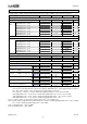
[AK4646] ■ Ordering Guide −30 ∼ +85°C 32pin QFN (0.5mm pitch) −30 ∼ +85°C 32pin QFN (0.
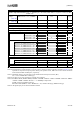
[AK4646] ■ Comparison with AK4642/AK4643 1. Function Function AVDD DVDD Power Supply for SPK-Amp Output Voltage of MIC Power MIC-Amp HPF / LPF Notch filter ALC Recovery Operation Waiting Period Read of ALC Volume Output Volume AK4642 AK4643 2.6V ∼ 3.6V 2.6V ∼ 3.6V 2.6V ∼ 5.25V (HVDD) 0.75 x AVDD AK4646 2.2V ∼ 3.6V 1.6V ∼ 3.6V 2.2V ∼ 4.0V (SVDD) 0.
[AK4646] PIN/FUNCTION No. 1 Pin Name MPWR I/O O 2 VCOM O 3 4 AVSS AVDD - 5 VCOC O 6 NC - 7 PDN I 8 9 10 11 12 13 14 15 16 17 18 19 20 21 22 23 24 25 26 27 28 CSN CCLK CDTIO SDTI SDTO LRCK BICK DVDD DVSS MCKI MCKO SPN SPP SVDD SVSS NC I I I/O I O I/O I/O I O O O - Function MIC Power Supply Pin Common Voltage Output Pin, 0.5 x AVDD Bias voltage of ADC inputs and DAC outputs.
[AK4646] ■ Handling of Unused Pin The unused I/O pins should be processed appropriately as below. Classification Analog Digital Pin Name MPWR, VCOC, SPN, SPP, ROUT, LOUT, MIN, RIN2/IN2−, LIN2/IN2+, LIN1/IN1−, RIN1/IN1+ MCKO MCKI MS0557-E-06 Setting These pins should be open. This pin should be open. This pin should be connected to DVSS.
[AK4646] ABSOLUTE MAXIMUM RATINGS (AVSS=DVSS=SVSS=0V; Note 3) Parameter Symbol min max Units Power Analog AVDD 4.6 V −0.3 Supplies: Digital DVDD 4.6 V −0.3 Speaker-Amp SVDD 4.6 V −0.3 |AVSS – DVSS| (Note 4) 0.3 V ΔGND1 |AVSS – SVSS| (Note 4) 0.3 V ΔGND2 Input Current, Any Pin Except Supplies IIN mA ±10 Analog Input Voltage (Note 5) VINA AVDD+0.3 V −0.3 Digital Input Voltage (Note 6) VIND DVDD+0.3 V −0.
[AK4646] ANALOG CHARACTERISTICS (Ta=25°C; AVDD=DVDD=SVDD=3.3V; AVSS=DVSS=SVSS=0V; fs=44.
[AK4646] min typ max Units Parameter DAC Characteristics: Resolution 16 Bits Stereo Line Output Characteristics: DAC → LOUT, ROUT pins, ALC=OFF, OVOL=0dB, LOVL1-0 bit = “00”, RL=10kΩ Output Voltage (Note 17) LOVL1-0 bit = “00” 1.78 1.98 2.18 Vpp LOVL1-0 bit = “01” 2.25 2.50 2.75 Vpp S/(N+D) (−3dBFS) 78 88 dBFS S/N (A-weighted) 82 92 dB Interchannel Isolation 85 100 dB Interchannel Gain Mismatch 0.1 0.
[AK4646] min typ max Units Parameter Speaker-Amp Characteristics: DAC → SPP/SPN pins, ALC=OFF,OVOL=0dB, CL=3μF, Rserial=10Ω x 2, BTL, SVDD=3.8V Output SPKG1-0 bits = “11”, -0.5dBFS 6.33 Vpp Voltage (Note 18) S/(N+D) SPKG1-0 bits = “11”, -0.5dBFS 60 dB (Note 19) S/N (A-weighted) 90 dB Load Impedance (Note 20) 50 Ω Load Capacitance (Note 20) 3 μF Mono Input: MIN pin (External Input Resistance=20kΩ) Maximum Input Voltage (Note 21) 1.98 Vpp Gain (Note 22) MIN Æ LOUT/ROUT LOVL1-0 bit = “00” -4.5 0 +4.
[AK4646] FILTER CHARACTERISTICS (Ta = 25°C; AVDD =2.2 ∼ 3.6V, DVDD =1.6 ∼ 3.6V, SVDD =2.2 ∼ 4.0V; fs=44.1kHz; DEM=OFF) Parameter Symbol min typ max Units ADC Digital Filter (Decimation LPF): Passband (Note 25) PB 0 17.3 kHz ±0.16dB 19.4 kHz −0.66dB 19.9 kHz −1.1dB 22.1 kHz −6.9dB Stopband SB 26.1 kHz Passband Ripple PR dB ±0.1 Stopband Attenuation SA 73 dB Group Delay (Note 26) GD 19 1/fs Group Delay Distortion 0 ΔGD μs DAC Digital Filter (LPF): Passband (Note 25) PB 0 20.0 kHz ±0.05dB 22.05 kHz −6.
[AK4646] SWITCHING CHARACTERISTICS (Ta = 25°C; AVDD =2.2 ∼ 3.6V, DVDD =1.6 ∼ 3.6V, SVDD =2.2 ∼ 4.0V; CL=20pF) Parameter Symbol min typ PLL Master Mode (PLL Reference Clock = MCKI pin) MCKI Input Timing Frequency fCLK 12 Pulse Width Low tCLKL 0.4/fCLK Pulse Width High tCLKH 0.4/fCLK MCKO Output Timing Frequency fMCK 0.2352 Duty Cycle Except 256fs at fs=32kHz, 29.4kHz dMCK 40 50 256fs at fs=32kHz, 29.4kHz dMCK 33 LRCK Output Timing Frequency fs 7.
[AK4646] Parameter Symbol PLL Slave Mode (PLL Reference Clock = LRCK pin) LRCK Input Timing Frequency fs Duty Duty BICK Input Timing Period tBCK Pulse Width Low tBCKL Pulse Width High tBCKH PLL Slave Mode (PLL Reference Clock = BICK pin) LRCK Input Timing Frequency fs Duty Duty BICK Input Timing Period tBCK PLL3-0 bits = “0010” tBCK PLL3-0 bits = “0011” Pulse Width Low tBCKL Pulse Width High tBCKH External Slave Mode MCKI Input Timing Frequency 256fs fCLK 512fs fCLK 1024fs fCLK Pulse Width Low tCLKL Pulse
[AK4646] Parameter Symbol min Audio Interface Timing Master Mode tMBLR −40 BICK “↓” to LRCK Edge (Note 27) tLRD LRCK Edge to SDTO (MSB) −70 (Except I2S mode) tBSD BICK “↓” to SDTO −70 SDTI Hold Time tSDH 50 SDTI Setup Time tSDS 50 Slave Mode tLRB 50 LRCK Edge to BICK “↑” (Note 27) tBLR 50 BICK “↑” to LRCK Edge (Note 27) tLRD LRCK Edge to SDTO (MSB) (Except I2S mode) tBSD BICK “↓” to SDTO SDTI Hold Time tSDH 50 SDTI Setup Time tSDS 50 Control Interface Timing CCLK Period tCCK 200 CCLK Pulse Width Low tCCKL
[AK4646] ■ Timing Diagram 1/fCLK VIH MCKI VIL tCLKH tCLKL 1/fs 50%DVDD LRCK tLRCKH tLRCKL 1/fMCK Duty = tLRCKH x fs x 100 tLRCKL x fs x 100 50%DVDD MCKO tMCKL dMCK = tMCKL x fMCK x 100 Note 31. MCKO is not available at EXT Master mode. Figure 2. Clock Timing (PLL / EXT Master mode) 50%DVDD LRCK tBLR tBCKL BICK 50%DVDD tDLR tBSD SDTO 50%DVDD tSDS tSDH VIH SDTI VIL Figure 3.
[AK4646] 1/fCLK VIH MCKI VIL tCLKH tCLKL 1/fs VIH LRCK VIL tLRCKH tLRCKL tBCK Duty = tLRCKH x fs x 100 = tLRCKL x fs x 100 VIH BICK VIL tBCKH tBCKL fMCK 50%DVDD MCKO tMCKL dMCK = tMCKL x fMCK x 100 Figure 4. Clock Timing (PLL Slave mode; PLL Reference Clock = MCKI pin) 1/fCLK VIH MCKI VIL tCLKH tCLKL 1/fs VIH LRCK VIL tLRCKH tLRCKL Duty = tLRCKH x fs x 100 tLRCKL x fs x 100 tBCK VIH BICK VIL tBCKH tBCKL Figure 5.
[AK4646] VIH LRCK VIL tLRB tBLR VIH BICK VIL tBSD tLRD SDTO 50%DVDD MSB tSDH tSDS VIH SDTI VIL Figure 6. Audio Interface Timing (PLL/EXT Slave mode) VIH CSN VIL tCSH tCCKL tCSS tCCKH VIH CCLK VIL tCCK tCDH tCDS VIH CDTIO C1 C0 R/W VIL Figure 7. WRITE Command Input Timing tCSW VIH CSN VIL tCSH tCSS VIH CCLK VIL VIH CDTIO D2 D1 D0 VIL Figure 8.
[AK4646] VIH CSN VIL VIH CCLK Clock, H or L tCCZ tDCD CDTIO D3 VIL D2 D1 D0 Hi-Z 50% DVDD Figure 9. Read Data Output Timing PMADL bit or PMADR bit tPDV SDTO 50%DVDD Figure 10. Power Down & Reset Timing 1 tPD PDN VIL Figure 11.
[AK4646] OPERATION OVERVIEW ■ System Clock There are the following five clock modes to interface with external devices (Table 1 and Table 2). Mode PMPLL bit M/S bit PLL3-0 bits Figure PLL Master Mode (Note 32) 1 1 Table 4 Figure 12 PLL Slave Mode 1 Table 4 Figure 13 1 0 (PLL Reference Clock: MCKI pin) PLL Slave Mode 2 Figure 14 Table 4 1 0 Figure 15 (PLL Reference Clock: LRCK or BICK pin) EXT Slave Mode 0 0 x Figure 16 EXT Master Mode 0 1 x Figure 17 Note 32.
[AK4646] ■ PLL Mode When PMPLL bit is “1”, a fully integrated analog phase locked loop (PLL) generates a clock that is selected by the PLL3-0 and FS3-0 bits. The PLL lock time is shown in Table 4, when the AK4646 is supplied stable clocks after PLL is powered-up (PMPLL bit = “0” → “1”) or when the sampling frequency is changed.
[AK4646] ■ PLL Unlock State 1) PLL Master Mode (PMPLL bit = “1”, M/S bit = “1”) In this mode, LRCK and BICK pins go to “L” and irregular frequency clock is output from MCKO pins at MCKO bit is “1” before the PLL goes to lock state after PMPLL bit = “0” Æ “1”. If MCKO bit is “0”, MCKO pin goes to “L” (Table 7). After the PLL is locked, a first period of LRCK and BICK may be invalid clock, but these clocks return to normal state after a period of 1/fs.
[AK4646] ■ PLL Master Mode (PMPLL bit = “1”, M/S bit = “1”) When an external clock (12MHz, 13.5MHz, 24MHz or 27MHz) is input to MCKI pin, the MCKO, BICK and LRCK clocks are generated by an internal PLL circuit. The MCKO output frequency is selected by PS1-0 bits (Table 9) and the output is enabled by MCKO bit. The BICK output frequency is selected between 32fs or 64fs, by BCKO bit (Table 10). 12MHz, 13.
[AK4646] ■ PLL Slave Mode (PMPLL bit = “1”, M/S bit = “0”) A reference clock of PLL is selected among the input clocks to MCKI, BICK or LRCK pin. The required clock for the AK4646 is generated by an internal PLL circuit. Input frequency is selected by PLL3-0 bits (Table 4). a) PLL reference clock: MCKI pin BICK and LRCK inputs should be synchronized with MCKO output. The phase between MCKO and LRCK dose not matter.
[AK4646] b) PLL reference clock: BICK or LRCK pin Sampling frequency corresponds to 7.35kHz to 48kHz by changing FS3-0 bits (Table 6). AK4646 DSP or μP MCKO MCKI BICK LRCK 32fs or 64fs 1fs BCLK LRCK SDTO SDTI SDTI SDTO Figure 14.
[AK4646] ■ EXT Slave Mode (PMPLL bit = “0”, M/S bit = “0”) When PMPLL bit is “0”, the AK4646 becomes EXT mode. Master clock can directly be inputted from MCKI pin, without the internal PLL circuit operation. This mode is compatible with I/F of the normal audio CODEC. The clocks required to operate this mode are MCKI (256fs, 512fs or 1024fs), LRCK (fs) and BICK (≥32fs). The master clock (MCKI) should be synchronized with LRCK. The phase between these clocks does not matter.
[AK4646] ■ EXT Master Mode (PMPLL bit = “0”, M/S bit = “1”) The AK4646 becomes EXT Master Mode by setting PMPLL bit = “0” and M/S bit = “1”. Master clock is input from MCKI pin, the internal PLL circuit is not operated. The clock required to operate is MCKI (256fs, 512fs or 1024fs). The input frequency of MCKI is selected by FS1-0 bits (Table 13). Mode 0 1 2 3 MCKI Input Sampling Frequency Frequency Range Don’t care 0 0 256fs 7.35kHz ∼ 48kHz Don’t care 0 1 1024fs 7.35kHz ∼ 13kHz Don’t care 1 0 512fs 7.
[AK4646] ■ System Reset Upon power-up, the PDN pin should be “L” and be changed from “L” to “H” after all power supply are supplied. “L” time of 150ns or more is needed to reset in the AK4646. This ensures that all internal registers reset to their initial values. The ADC enters an initialization cycle that starts when the PMADL or PMADR bit is changed from “0” to “1”. The initialization cycle time is 1059/fs=24ms@fs=44.1kHz.
[AK4646] LRCK 0 1 2 3 9 10 11 12 13 14 15 0 1 2 3 9 10 11 12 13 14 15 0 1 BICK(32fs) SDTO(o) 15 14 13 7 6 5 4 3 2 1 0 15 14 13 7 6 5 4 3 2 1 0 15 SDTI(i) 15 14 13 7 6 5 4 3 2 1 0 15 14 13 7 6 5 4 3 2 1 0 15 0 1 2 3 15 16 17 18 31 0 1 2 3 15 16 17 18 31 0 1 BICK(64fs) SDTO(o) SDTI(i) 1 0 15 14 13 15 14 13 15 14 Don't Care 1 0 1 0 Don't Care 15 15 14 2 1 0 15:MSB, 0:LSB Lch Data Rch Data Figure 18.
[AK4646] LRCK 0 1 2 3 9 10 11 12 13 14 15 0 1 2 3 9 10 11 12 13 14 15 0 1 BICK(32fs) SDTO(o) 0 15 14 8 7 6 5 4 3 2 1 0 15 14 8 7 6 5 4 3 2 1 0 SDTI(i) 0 15 14 8 7 6 5 4 3 2 1 0 15 14 8 7 6 5 4 3 2 1 0 0 1 2 3 15 16 17 18 31 0 1 2 3 15 16 17 18 31 0 1 BICK(64fs) SDTO(o) 15 14 2 1 0 SDTI(i) 15 14 2 1 0 Don't Care 15 14 2 1 0 15 14 2 1 0 Don't Care 15:MSB, 0:LSB Lch Data Rch Data Figure 20. Mode 3 Timing ■ Mono/Stereo Mode PMADL and PMADR bits set mono/stereo ADC operation.
[AK4646] ■ MIC/LINE Input Selector The AK4646 has an input selector. When MDIF1 and MDIF2 bits are “0”, INL and INR bits select LIN1/LIN2 and RIN1/RIN2, respectively. When MDIF1 and MDIF2 bits are “1”, LIN1, RIN1, LIN2 and RIN2 pins become IN1−, IN1+, IN2+ and IN2− pins respectively. In this case, full-differential input is available (Figure 22).
[AK4646] ■ MIC Gain Amplifier The AK4646 has a gain amplifier for microphone input. The gain of MIC-Amp is selected by the MGAIN2-0 bits (Table 19). The typical input impedance is 30kΩ (typ). MGAIN2 bit 0 0 0 0 1 1 1 1 MGAIN1 bit MGAIN0 bit Input Gain 0 0 0dB 0 1 +20dB 1 0 +26dB 1 1 +32dB 0 0 +10dB 0 1 +17dB 1 0 +23dB 1 1 +29dB Table 19. Mic Input Gain (default) ■ MIC Power When PMMP bit = “1”, the MPWR pin supplies power for the microphone. This output voltage is typically 0.
[AK4646] ■ Digital Block The digital block consists of block diagram as shown in Figure 24. HPF ~ ALC blocks are used for recording path when DAFIL bit = “0” and either ADC (Lch or Rch) is powered-up. Also HPF ~ ALC blocks are used for playback path when DAFIL bit = “1” or both ADC (Lch and Rch) are powered-down (Figure 24 ~ Figure 27, Table 21). The SDTO pin outputs “L” when DAFIL bit = “1”, even if ADC is powered-up.
[AK4646] PMADL PMADR PMDAC DAFIL bit 1 1 0 0 x 1 1 0 bit 1 0 1 0 x 1 0 1 bit x x x 1 1 1 1 1 bit 0 0 0 0 1 0 0 0 Mode Recording Mode Playback Mode Loop Through Mode LOOP bit 0 0 0 0 0 1 1 1 Figure 24 SW SW1 SW2 1 0 1 0 1 0 0 1 0 1 1 1 1 1 1 1 Figure Figure 25 Figure 26 Figure 27 (x: Don’t Care) Table 21. Recording Playback Mode LPF bit, HPF bit, FIL3 bit, EQ0 bit, EQ1 bit, EQ2 bit, EQ3 bit, EQ4 bit, EQ5 bit, ACL1 bit and ALC2 bit should be “0” when selecting those modes.
[AK4646] ■ Digital Programmable Filter Circuit (1) High Pass Filter (HPF) Normally, this HPF is used for a Wind-Noise Reduction Filter. This is composed with 2 steps of 1st order HPF. The coefficient of both HPF is the same and set by F1A13-0 bits and F1B13-0 bits. HPFAD bit controls ON/OFF of the 1st step HPF and HPF bit controls ON/OFF of the 2nd step HPF. When the HPF is OFF, the audio data passes this block by 0dB gain.
[AK4646] (3) Stereo Separation Emphasis Filter (FIL3) FIL3 is used to emphasize the stereo separation of stereo mic recording data or playback data. F3A13-0 and F3B13-0 bits set the filter coefficient of FIL3. FIL3 becomes High Pass Filter (HPF) at F3AS bit = “0”, and Low Pass Filter (LPF) at F3AS bit = “1”. FIL3 bit controls ON/OFF of FIL3. When Stereo Separation Emphasis Filter is OFF, the audio data passes this block by 0dB gain.
[AK4646] (4) Gain Compensation (EQ0) Gain Compensation is used to compensate the frequency response and the gain that is changed by Stereo Separation Emphasis Filter. Gain Compensation is composed of the Equalizer (EQ0) and the Gain (0dB/+12dB/+24dB). E0A15-0, E0B13-0 and E0C15-0 bits set the coefficient of EQ0. GN1-0 bits set the gain (Table 22). EQ0 bit controls ON/OFF of EQ0. When EQ is OFF and the gain is 0dB, the audio data passes this block by 0dB gain.
[AK4646] (5) 5-band Notch This block can be used as Equalizer or Notch Filter. 5-band Equalizer (EQ1, EQ2, EQ3, EQ4 and EQ5) is selected ON/OFF independently by EQ1, EQ2, EQ3, EQ4 and EQ5 bits. When Equalizer is OFF, the audio data passes this block by 0dB gain. E1A15-0, E1B15-0 and E1C15-0 bits set the coefficient of EQ1. E2A15-0, E2B15-0 and E2C15-0 bits set the coefficient of EQ2. E3A15-0, E3B15-0 and E3C15-0 bits set the coefficient of EQ3. E4A15-0, E4B15-0 and E4C15-0 bits set the coefficient of EQ4.
[AK4646] ■ ALC Operation The ALC (Automatic Level Control) is operated by ALC block when ALC bit is “1”. When both Lch and Rch of ADC are powered-down or DAFIL bit is “1”, ALC circuit operates at playback path. When either Lch and Rch of ADC is powered-up and DAFIL bit is “0”, ALC circuit operates at recording path. Note 37. In this section, VOL means IVL and IVR for recording path, OVL and OVR for playback path. Note 38.
[AK4646] 2. ALC Recovery Operation The ALC recovery operation waits for the WTM2-0 bits (Table 26) to be set after completing the ALC limiter operation. If the input signal does not exceed “ALC recovery waiting counter reset level” (Table 23) during the wait time, the ALC recovery operation is done. The VOL value is automatically incremented by RGAIN1-0 bits (Table 27) up to the set reference level (Table 28) with zero crossing detection which timeout period is set by ZTM1-0 bits (Table 25).
[AK4646] IREF7-0bits GAIN(0dB) Step F1H +36.0 F0H +35.625 EFH +35.25 : : E1H +30.0 (default) 0.375dB : : 92H +0.375 91H 0.0 90H -0.375 : : 2H -53.625 1H -54.0 0H MUTE Table 28. Reference Level at ALC Recovery operation for recoding OREF5-0bits GAIN(0dB) Step 3CH +36.0 3BH +34.5 3AH +33.0 : : 28H +6.0 (default) 1.5dB : : 25H +1.5 24H 0.0 23H -1.5 : : 2H -51.0 1H -52.5 0H -54.0 Table 29.
[AK4646] 3. The Volume at the ALC Operation The current volume value at the ALC operation is reflected by VOL7-0 bits. It is enable to check the current volume value with reading the register value of VOL7-0 bits. VOL7-0bits GAIN(0dB) F1H +36.0 F0H +35.625 EFH +35.25 : : C5H +19.5 : : 92H +0.375 91H 0.0 90H -0.375 : : 2H -53.625 1H -54.0 0H MUTE Table 31. Value of VOL7-0 bits 4. Example of ALC Operation Table 32 and Table 33 show the examples of the ALC setting for recording and playback path.
[AK4646] Register Name Comment LMTH1-0 ZELMN ZTM1-0 Limiter detection Level Limiter zero crossing detection Zero crossing timeout period Recovery waiting period *WTM2-0 bits should be the same data as ZTM1-0 bits Maximum gain at recovery operation WTM2-0 OREF5-0 OVL7-0, OVR7-0 LMAT1-0 LFST RGAIN1-0 RFST1-0 ALC2 Data 01 0 01 Gain of VOL fs=8kHz Operation −4.1dBFS Enable 32ms Data 01 0 11 fs=44.1kHz Operation −4.1dBFS Enable 23.2ms 001 32ms 100 46.
[AK4646] ■ Input Digital Volume (Manual Mode) The input digital volume becomes a manual mode at ALC1 bit = “0” when either Lch and Rch of ADC is powered-up (PMADL bit = “1” or PMADR bit = “1”) and DAFIL bit is “0”. This mode is used in the case shown below. 1. 2. 3. After exiting reset state, set-up the registers for the ALC operation (ZTM1-0, LMTH and etc) When the registers for the ALC operation (Limiter period, Recovery period and etc) are changed.
[AK4646] ■ Output Digital Volume (Manual Mode) The ALC block becomes output digital volume (manual mode) by setting ALC2 bit to “0” when both Lch and Rch of ADC are powered-down (PMADL = PMADR bits = “1”) or DAFIL bit is “1”. The output digital volume gain is set by the OVL7-0 bit and the OVR7-0 bit (Table 35). When the OVOLC bit = “1”, the OVL7-0 bits control both Lch and Rch volume levels. When the OVOLC bit = “0”, the OVL7-0 bits control Lch level and the OVR7-0 bits control Rch level.
[AK4646] ■ De-emphasis Filter The AK4646 includes the digital de-emphasis filter (tc = 50/15μs) which corresponds 3 kinds frequency (32kHz, 44kHz, 48kHz) by IIR filter. Setting the DEM1-0 bits enables the de-emphasis filter (Table 37). DEM1 0 0 1 1 DEM0 Mode 0 44.1kHz 1 OFF (default) 0 48kHz 1 32kHz Table 37. De-emphasis Control ■ Soft Mute Soft mute operation is performed in the digital input domain.
[AK4646] ■ Analog Mixing: Mono Input When the PMBP bit is set to “1”, the mono input is powered-up. When the BEEPS bit is set to “1”, the input signal from the MIN pin is output to Speaker-Amp. When the BEEPH bit is set to “1”, the input signal from the MIN pin is output to Headphone-Amp. When the BEEPL bit is set to “1”, the input signal from the MIN pin is output to the stereo line output amplifier. The external resister Ri adjusts the signal level of MIN input.
[AK4646] ■ Stereo Line Output (LOUT/ROUT pins) When DACL bit is “1”, Lch/Rch signal of DAC is output from the LOUT/ROUT pins which is single-ended. When DACL bit is “0”, output signal is muted and LOUT/ROUT pins output VCOM voltage. The load impedance is 10kΩ (min.). When the PMLO bit = LOPS bit = “0”, the stereo line output enters power-down mode and the output is pulled-down to AVSS by 100kΩ(typ). When the LOPS bit is “1”, stereo line output enters power-save mode.
[AK4646] [Stereo Line Output Control Sequence (in case of using Pop Reduction Circuit)] (2 ) (5 ) P M L O b it (1 ) (3 ) (4 ) (6 ) L O P S b it L O U T , R O U T p in s N o r m a l O u tp u t ≥ 300 m s ≥ 300 m s Figure 33. Stereo Line Output Control Sequence (in case of using Pop Reduction Circuit) (1) Set LOPS bit = “1”. Stereo line output enters the power-save mode. (2) Set PMLO bit = “1”. Stereo line output exits the power-down mode. LOUT and ROUT pins rise up to VCOM voltage.
[AK4646] ■ Speaker Output Power supply for Speaker-Amp (SVDD) is 2.2V to 4.0V. In case of dynamic (electromagnetic) speaker (load resistance < 50Ω), SVDD is 2.2V to 3.6V. Speaker Type Dynamic Speaker Piezo (Ceramic) Speaker Load Resistance (min) 50Ω (Note 20) 8Ω Load Capacitance (max) 30pF 3μF (Note 20) Note 20. Load impedance is total impedance of series resistance and piezo speaker impedance at 1kHz in 38HFigure 34. Load capacitance is capacitance of piezo speaker.
[AK4646] When a piezo speaker is used, resistances more than 10Ω should be inserted between SPP/SPN pins and speaker in series, respectively, as shown in Figure 34. Zener diodes should be inserted between speaker and GND as shown in Figure 34, in order to protect SPK-Amp of AK4646 from the power that the piezo speaker outputs when the speaker is pressured. Zener diodes of the following zener voltage should be used. 0.
[AK4646] Speaker-Amp is powered-up/down by PMSPK bit. When PMSPK bit is “0”, both SPP and SPN pins are in Hi-Z state. When PMSPK bit is “1” and SPPSN bit is “0”, the Speaker-Amp enters power-save mode. In this mode, SPP pin is placed in Hi-Z state and SPN pin goes to SVDD/2 voltage. When the PMSPK bit is “1” after PDN pin is controlled from “L” to “H”, the SPP and SPN pins rise up from power-save-mode.
[AK4646] ■ Serial Control Interface Internal registers may be written by using the 3-wire µP interface pins (CSN, CCLK and CDTIO). The data on this interface consists of Read/Write, Register address (MSB first, 7bits) and Control data (MSB first, 8bits). Each bit is clocked in on the rising edge (“↑”) of CCLK. It is available for writing data on the rising edge of CSN. When reading operation, CDTIO pin has become an output mode at the falling edge of 8th CCLIC and outputs D7-D0.
[AK4646] ■ Register Map Addr 00H 01H 02H 03H 04H 05H 06H 07H 08H 09H 0AH 0BH 0CH 0DH 0EH 0FH 10H 11H 12H 13H 14H 15H 16H 17H 18H 19H 1AH 1BH 1CH 1DH 1EH 1FH 20H 21H 22H 23H 24H 25H 26H 27H 28H 29H 2AH 2BH 2CH 2DH 2EH 2FH Register Name Power Management 1 Power Management 2 Signal Select 1 Signal Select 2 Mode Control 1 Mode Control 2 Timer Select ALC Mode Control 1 ALC Mode Control 2 Lch Input Volume Control Output Volume Control ALC Mode Control 3 Rch Input Volume Control ALC LEVEL Mode Control 3 Mode Con
[AK4646] Addr 30H 31H 32H 33H 34H 35H 36H 37H 38H 39H 3AH 3BH 3CH 3DH 3EH 3FH 40H 41H 42H 43H 44H 45H 46H 47H 48H 49H 4AH 4BH 4CH 4DH 4EH 4FH Register Name Digital Filter Select 2 Reserved E1 Co-efficient 0 E1 Co-efficient 1 E1 Co-efficient 2 E1 Co-efficient 3 E1 Co-efficient 4 E1 Co-efficient 5 E2 Co-efficient 0 E2 Co-efficient 1 E2 Co-efficient 2 E2 Co-efficient 3 E2 Co-efficient 4 E2 Co-efficient 5 E3 Co-efficient 0 E3 Co-efficient 1 E3 Co-efficient 2 E3 Co-efficient 3 E3 Co-efficient 4 E3 Co-efficient
[AK4646] ■ Register Definitions Addr 00H Register Name Power Management 1 R/W Default D7 0 R 0 D6 PMVCM R/W 0 D5 PMBP R/W 0 D4 PMSPK R/W 0 D3 PMLO R/W 0 D2 PMDAC R/W 0 D1 0 R 0 D0 PMADL R/W 0 PMADL: MIC-Amp Lch and ADC Lch Power Management 0: Power-down (default) 1: Power-up When the PMADL or PMADR bit is changed from “0” to “1”, the initialization cycle (1059/fs=24ms @44.1kHz) starts. After initializing, digital data of the ADC is output.
[AK4646] Addr 01H Register Name Power Management 2 R/W Default D7 0 R 0 D6 0 R 0 D5 0 R 0 D4 0 R 0 D3 M/S R/W 0 D2 0 R 0 D3 0 R 0 D2 PMMP R/W 0 D1 MCKO R/W 0 D0 PMPLL R/W 0 PMPLL: PLL Power Management 0: EXT Mode and Power-Down (default) 1: PLL Mode and Power-up MCKO: Master Clock Output Enable 0: Disable: MCKO pin = “L” (default) 1: Enable: Output frequency is selected by PS1-0 bits.
[AK4646] Addr 03H Register Name Signal Select 2 R/W Default D7 DAFIL R/W 0 D6 LOPS R/W 0 D5 MGAIN1 R/W 0 D4 SPKG1 R/W 0 D3 SPKG0 R/W 0 D2 BEEPL R/W 0 D1 LOVL1 R/W 0 D0 LOVL0 R/W 0 LOVL1-0: Output Stereo Line Gain Select (Table 41) Default: 00(0dB) BEEPL: Switch Control from MIN pin to Stereo Line Output 0: OFF (default) 1: ON When PMLO bit is “1”, BEEPL bit is enabled. When PMLO bit is “0”, the LOUT/ROUT pins go to AVSS.
[AK4646] Addr 06H Register Name Timer Select R/W Default D7 0 R 0 D6 WTM2 R/W 0 D5 ZTM1 R/W 0 D4 ZTM0 R/W 0 D3 WTM1 R/W 0 D2 WTM0 R/W 0 D1 RFST1 R/W 0 D0 RFST0 R/W 0 WTM2-0: ALC Recovery Waiting Period (Table 26) A period of recovery operation when any limiter operation does not occur during the ALC1 operation Default is “000” (128/fs).
[AK4646] Addr 08H Register Name ALC Mode Control 2 R/W Default D7 IREF7 R/W 1 D6 IREF6 R/W 1 D5 IREF5 R/W 1 D4 IREF4 R/W 0 D3 IREF3 R/W 0 D2 IREF2 R/W 0 D1 IREF1 R/W 0 D0 IREF0 R/W 1 REF7-0: Reference Value at ALC Recovery Operation. 0.375dB step, 242 Level (Table 28) Default: “E1H” (+30.
[AK4646] Addr 0EH Register Name Mode Control 3 R/W Default D7 READ R/W 0 D6 LOOP R/W 0 D5 SMUTE R/W 0 D4 OVOLC R/W 1 D3 DATT1 R/W 0 D2 DATT0 R/W 0 D1 DEM1 R/W 0 D0 DEM0 R/W 1 DEM1-0: De-emphasis Frequency Select (Table 37) Default: “01” (OFF) DATT1-0: Output Digital Volume2; 6dB step, 4 Level (Table 36) Default: “00H” (0.
[AK4646] Addr 10H Register Name Power Management 3 R/W Default D7 0 R 0 D6 0 R 0 D5 0 R 0 D4 MDIF2 R/W 0 D3 MDIF1 R/W 0 D2 INR R/W 0 D1 INL R/W 0 D0 PMADR R/W 0 D4 HPF R/W 0 D3 EQ0 R/W 0 D2 FIL3 R/W 0 D1 0 R 0 D0 HPFAD R/W 1 PMADR: MIC-Amp Lch and ADC Rch Power Management 0: Power-down (default) 1: Power-up INL: ADC Lch Input Source Select 0: LIN1 pin (default) 1: LIN2 pin INR: ADC Rch Input Source Select 0: RIN1 pin (default) 1: RIN2 pin MDIF1: ADC Lch Input Type Select 0: Single-ended inpu
[AK4646] LPF: LPF Coefficient Setting Enable 0: Disable (default) 1: Enable When LPF bit is “1”, the settings of F2A13-0 and F2B13-0 bits are enabled. When LPF bit is “0”, LPF block is through (0dB).
[AK4646] Addr 30H Register Name Digital Filter Select 2 R/W Default D7 0 R 0 D6 0 R 0 D5 0 R 0 D4 EQ5 R/W 0 D3 EQ4 R/W 0 D2 EQ3 R/W 0 D1 EQ2 R/W 0 D0 EQ1 R/W 0 EQ1: Equalizer 1 Coefficient Setting Enable 0: Disable (default) 1: Enable When EQ1 bit is “1”, the settings of E1A15-0, E1B15-0 and E1C15-0 bits are enabled. When EQ1 bit is “0”, EQ1 block is through (0dB).
[AK4646] Addr 32H 33H 34H 35H 36H 37H 38H 39H 3AH 3BH 3CH 3DH 3EH 3FH 40H 41H 42H 43H 44H 45H 46H 47H 48H 49H 4AH 4BH 4CH 4DH 4EH 4FH Register Name E1 Co-efficient 0 E1 Co-efficient 1 E1 Co-efficient 2 E1 Co-efficient 3 E1 Co-efficient 4 E1 Co-efficient 5 E2 Co-efficient 0 E2 Co-efficient 1 E2 Co-efficient 2 E2 Co-efficient 3 E2 Co-efficient 4 E2 Co-efficient 5 E3 Co-efficient 0 E3 Co-efficient 1 E3 Co-efficient 2 E3 Co-efficient 3 E3 Co-efficient 4 E3 Co-efficient 5 E4 Co-efficient 0 E4 Co-efficient 1 E4
[AK4646] SYSTEM DESIGN Figure 37 shows the system connection diagram for the AK4646. An evaluation board [AKD4646] is available which demonstrates the optimum layout, power supply arrangements and measurement results. Speaker 10u ZD2 Dynamic SPK R1, R2: Short ZD1, ZD2: Open Piezo SPK R1, R2: ≥10Ω ZD1, ZD2: Requi red Line Out 200 Mono In External MIC 1u 1u 23 22 21 20 19 18 17 NC SVSS SVDD SPP SPN MCKO MCKI R2 24 NC 20k 20k 200 R1 0.1u ZD1 10 Power Supply 2.2 ∼ 3.6V 0.
[AK4646] 1. Grounding and Power Supply Decoupling The AK4646 requires careful attention to power supply and grounding arrangements. AVDD, DVDD and SVDD are usually supplied from the system’s analog supply. If AVDD, DVDD and SVDD are supplied separately, the power-up sequence is not critical. AVSS, DVSS and SVSS of the AK4646 should be connected to the analog ground plane.
[AK4646] CONTROL SEQUENCE ■ Clock Set up When ADC or DAC is powered-up, the clocks must be supplied. 1. PLL Master Mode. Example: Power Supply Audio I/F Format: MSB justified (ADC & DAC) BICK frequency at Master Mode: 64fs Input Master Clock Select at PLL Mode: 11.2896MHz MCKO: Enable Sampling Frequency: 44.
[AK4646] 2. PLL Slave Mode (LRCK or BICK pin) Example: Power Supply Audio I/F Format : MSB justified (ADC & DAC) PLL Reference clock: BICK BICK frequency: 64fs Sampling Frequency: 44.1kHz (1) PDN pin (2) 4fs (1)ofPower Supply & PDN pin = “L” Æ “H” (3) PMVCM bit (Addr:00H, D6) PMPLL bit (2) Addr:04H, Data:32H Addr:05H, Data:27H (Addr:01H, D0) LRCK pin BICK pin Input (3) Addr:00H, Data:40H (4) Internal Clock (5) (4) Addr:01H, Data:01H Figure 39.
[AK4646] 3. PLL Slave Mode (MCKI pin) Example: Audio I/F Format: MSB justified (ADC & DAC) BICK frequency at Master Mode: 64fs Input Master Clock Select at PLL Mode: 11.
[AK4646] 4. EXT Slave Mode Example: Audio I/F Format: MSB justified (ADC and DAC) Input MCKI frequency: 1024fs MCKO: Disable Power Supply (1) Power Supply & PDN pin = “L” Æ “H” (1) PDN pin (2) (2) Addr:04H, Data:02H Addr:05H, Data:27H (3) PMVCM bit (Addr:00H, D6) (4) MCKI pin Input (3) Addr:00H, Data:40H (4) LRCK pin BICK pin Input MCKI, BICK and LRCK input Figure 41.
[AK4646] ■ MIC Input Recording (Stereo) Example: FS3-0 bits (Addr:05H, D5&D2-0) 0,000 PLL Master Mode Audio I/F Format:MSB justified (ADC & DAC) Pre MIC AMP:+20dB Sampling Frequency:44.
[AK4646] ■ Speaker-amp Output FS3-0 bits (Addr:05H, D5&D2-0) 0,000 1,111 Example: (1) PLL Master Mode Audio I/F Format: MSB justified (ADC & DAC) Sampling Frequency:44.
[AK4646] ■ Mono signal output from Speaker-Amp Example: Clocks can be stopped.
[AK4646] ■ Stereo Line Output FS3-0 bits (Addr:05H, D5&D2-0) Example: 1,111 0,000 PLL, Master Mode Audio I/F Format :MSB justified (ADC & DAC) Sampling Frequency:44.
[AK4646] ■ Stop of Clock Master clock can be stopped when ADC and DAC are not used. 1. PLL Master Mode Example: Audio I/F Format: MSB justified (ADC & DAC) BICK frequency at Master Mode: 64fs Input Master Clock Select at PLL Mode: 11.2896MHz (1) PMPLL bit (Addr:01H, D0) (2) MCKO bit "0" or "1" (1) (2) Addr:01H, Data:08H (Addr:01H, D1) (3) External MCKI Input (3) Stop an external MCKI Figure 46.
[AK4646] 3. PLL Slave (MCKI pin) Example (1) Audio I/F Format: MSB justified (ADC & DAC) PLL Reference clock: MCKI BICK frequency: 64fs PMPLL bit (Addr:01H, D0) (1) MCKO bit (1) Addr:01H, Data:00H (Addr:01H, D1) (2) External MCKI Input (2) Stop the external clocks Figure 48. Clock Stopping Sequence (3) (1) Power down PLL: PMPLL bit = “1” → “0” Stop MCKO output: MCKO bit = “1” → “0” (2) Stop the external master clock. 4.
[AK4646] PACKAGE (AK4646EN) 32pin QFN (Unit: mm) 5.00 ± 0.10 0.40 ± 0.10 4.75 ± 0.10 24 17 16 4.75 ± 0.10 B 3.5 5.00 ± 0.10 25 32 1 1 3.5 0.50 +0.07 -0.05 32 C0.42 8 A 0.23 Exposed Pad 9 0.85 ± 0.05 0.10 M AB 0.08 C 0.04 0.01+- 0.01 0.20 C Note) The exposed pad on the bottom surface of the package must be open or connected to the ground.
[AK4646] PACKAGE (AK4646EZ) 32pin QFN (Unit: mm) 4.0 ± 0.1 2.4 ± 0.1 17 24 0.40 ± 0.10 25 2.4 ± 0.1 4.0 ± 0.1 16 A Exposed Pad 32 9 0.45 ± 0.10 8 1 0.22 ± 0.05 B 0.18 ± 0.05 0.05 M C0.3 PIN #1 ID 0.65 MAX 0.4 0.00 MIN 0.05 MAX 0.08 Note) The exposed pad on the bottom surface of the package must be open or connected to the ground. Note that the maximum operating ambient temperature is 70°C when it is open.
[AK4646] MARKING (AK4646EN) AKM AK4646 XXXXX 1 XXXXX: Date code identifier (5 digits) MARKING (AK4646EZ) 4646 XXXX 1 XXXX: Date code identifier (4 digits) MS0557-E-06 2011/06 - 79 -
[AK4646] REVISION HISTORY Date (YY/MM/DD) Revision 07/05/14 02 10/01/07 03 10/08/19 04 11/01/19 05 11/06/22 06 Reason First Edition Specification Change Description Change Specification Addition Error Correction Page Contents 39, 40 53, 60 FR bit was added. (ALC fast recovery function enable bit) Error Correction 26 Descriptions about the AK4646EZ were added. 7 9 RECOMMENDED OPERATING CONDITIONS AVDD – SVDD was added: 0.8V (max) ANALOG CHARACTERISTICS Note 18 was changed.
[AK4646] IMPORTANT NOTICE z These products and their specifications are subject to change without notice. When you consider any use or application of these products, please make inquiries the sales office of Asahi Kasei Microdevices Corporation (AKM) or authorized distributors as to current status of the products.