
Datasheet

[AK4646]
MS0557-E-06 2011/06
- 21 -
■ PLL Unlock State
1) PLL Master Mode (PMPLL bit = “1”, M/S bit = “1”)
In this mode, LRCK and BICK pins go to “L” and irregular frequency clock is output from MCKO pins at MCKO bit is
“1” before the PLL goes to lock state after PMPLL bit = “0” Æ “1”. If MCKO bit is “0”, MCKO pin goes to “L” (
Table
7).
After the PLL is locked, a first period of LRCK and BICK may be invalid clock, but these clocks return to normal state
after a period of 1/fs.
When sampling frequency is changed, BICK and LRCK pins do not output irregular frequency clocks but go to “L” by
setting PMPLL bit to “0”.
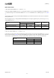
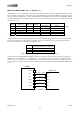
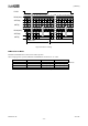
MCKO pin
PLL State
MCKO bit = “0” MCKO bit = “1”
BICK pin LRCK pin
After that PMPLL bit “0” Æ “1” “L” Output Invalid “L” Output “L” Output
PLL Unlock (except the case
above)
“L” Output Invalid Invalid Invalid
PLL Lock “L” Output Table 9 Table 10 1fs Output
Table 7. Clock Operation at PLL Master Mode (PMPLL bit = “1”, M/S bit = “1”)
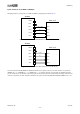
2) PLL Slave Mode (PMPLL bit = “1”, M/S bit = “0”)
In this mode, an invalid clock is output from MCKO pin before the PLL goes to lock state after PMPLL bit = “0” Æ “1”.
Then, the clock selected by
Table 9 is output from MCKO pin when PLL is locked. ADC and DAC output invalid data
when the PLL is unlocked. For DAC, the output signal should be muted by writing “0” to DACL and DACS bits.
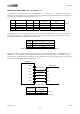
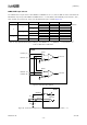
MCKO pin
PLL State
MCKO bit = “0” MCKO bit = “1”
After that PMPLL bit “0” Æ “1” “L” Output Invalid
PLL Unlock “L” Output Invalid
PLL Lock “L” Output Output
Table 8. Clock Operation at PLL Slave Mode (PMPLL bit = “0”, M/S bit = “0”)